SLVSFP3C August   2020  – March 2022 TPS61288

PRODUCTION DATA  

  1. Features
  2. Applications
  3. Description
  4. Revision History
  5. Device Comparison
  6. Pin Configuration and Functions
  7. Specifications
    1. 7.1 Absolute Maximum Ratings
    2. 7.2 ESD Ratings
    3. 7.3 Recommended Operating Conditions
    4. 7.4 Thermal Information
    5. 7.5 Electrical Characteristics
    6. 7.6 Typical Characteristics
  8. Detailed Description
    1. 8.1 Overview
    2. 8.2 Functional Block Diagram
    3. 8.3 Feature Description
      1. 8.3.1 Enable and Start-up
      2. 8.3.2 Undervoltage Lockout (UVLO)
      3. 8.3.3 Switching Peak Current Limit
      4. 8.3.4 Overvoltage Protection
      5. 8.3.5 Thermal Shutdown
    4. 8.4 Device Functional Modes
      1. 8.4.1 PWM
      2. 8.4.2 PFM
  9. Application and Implementation
    1. 9.1 Application Information
    2. 9.2 Typical Application
      1. 9.2.1 Design Requirements
      2. 9.2.2 Detailed Design Procedure
        1. 9.2.2.1 Setting Output Voltage
        2. 9.2.2.2 Inductor Selection
        3. 9.2.2.3 Input Capacitor Selection
        4. 9.2.2.4 Output Capacitor Selection
        5. 9.2.2.5 Loop Stability
      3. 9.2.3 Application Curves
  10. 10Power Supply Recommendations
  11. 11Layout
    1. 11.1 Layout Guidelines
    2. 11.2 Layout Example
      1. 11.2.1 Thermal Considerations
  12. 12Device and Documentation Support
    1. 12.1 Receiving Notification of Documentation Updates
    2. 12.2 Support Resources
    3. 12.3 Trademarks
    4. 12.4 Electrostatic Discharge Caution
    5. 12.5 Glossary
  13. 13Mechanical, Packaging, and Orderable Information

Package Options

Mechanical Data (Package|Pins)
Thermal pad, mechanical data (Package|Pins)
Orderable Information

Typical Characteristics

TA = 25°C, fSW = 500 kHz, unless otherwise noted.
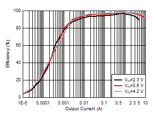
TA = 25°C, fSW = 500 kHz, unless otherwise noted.GUID-20201119-CA0I-FZG2-DBCK-KC1HZNZNBBJ2-low.gif
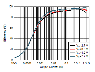
VIN = 2.7 V; 3.6 V; 4.2 V; 7.2 V VOUT = 13 V
Figure 7-1 Efficiency vs Output Current VOUT = 13 V. TA = 25°C, fSW = 500 kHz, unless otherwise noted.
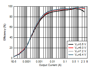
GUID-20201119-CA0I-GMF1-GWZG-9MMSGX8R7FRJ-low.gif
VIN = 3.6 V; 6 V; 7.2 V; 8.4 V VOUT = 16 V
Figure 7-3 Efficiency vs Output Current, VOUT = 16 V
GUID-20201119-CA0I-9XC8-TGLJ-C7H8JKFFLRC7-low.gif
Separate power VIN and 3.3 V signal VIN VOUT = 5.5 V
Figure 7-5 Efficiency vs Output Current, VOUT = 5.5 V
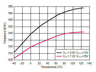
GUID-20201116-CA0I-0RS3-VP0C-RXQH401T6DDS-low.gif
Figure 7-7 Switching Frequency vs Temperature
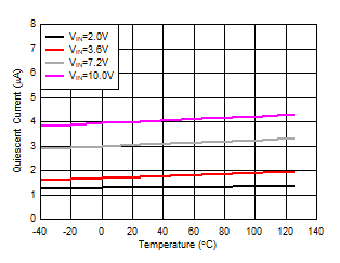
GUID-20201116-CA0I-LWPM-MGWH-R7VPHJDKDXZK-low.gif
VIN = 2.0 V; 3.6 V; 7.2 V; 10 V VOUT = 13 V
Figure 7-9 Quiescent Current into VIN vs Temperature
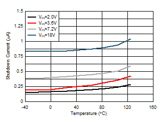
GUID-20201116-CA0I-ZHQK-RDXN-JB2G9NGHD28C-low.gif
Figure 7-11 Shutdown Current vs Temperature
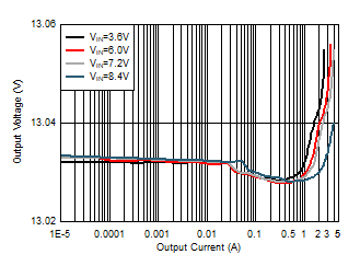
GUID-20201119-CA0I-P3LZ-JCVT-F2GNT8BHQXZD-low.gif
VIN = 2.7 V; 3.6 V; 4.2 V; 7.2 V VOUT = 13 V
Figure 7-2 Output Voltage vs Output Current, VOUT = 13 V
GUID-20201119-CA0I-P3LZ-JCVT-F2GNT8BHQXZD-low.gif
VIN = 3.6 V; 6 V; 7.2 V; 8.4 V VOUT = 16 V
Figure 7-4 Output Voltage vs Output Current, VOUT = 16 V
GUID-20201119-CA0I-JR2F-7SLN-NWLRR9PGWZ4R-low.gif
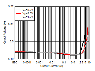
Separate power VIN and 3.3 V signal VIN VOUT = 5.5 V
Figure 7-6 Output Voltage vs Output Current, VOUT = 5.5 V
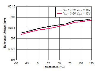
GUID-20201116-CA0I-B67J-MCHX-2TD8ZG4PWP3Q-low.gif
Figure 7-8 Reference Voltage vs Temperature
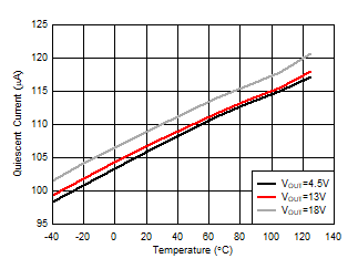
GUID-20201116-CA0I-F2CJ-3KG1-BSXZK4C1WG9D-low.gif
VIN = 3.6 V VOUT = 4.5 V; 13 V; 18 V
Figure 7-10 Quiescent Current into VOUT vs Temperature