SLVSGQ1B January 2022 – January 2024 TPS61376
PRODUCTION DATA
- 1
- 1 Features
- 2 Applications
- 3 Description
- 4 Pin Configuration and Functions
- 5 Specifications
-
6 Detailed Description
- 6.1 Overview
- 6.2 Functional Block Diagram
- 6.3
Feature Description
- 6.3.1 VCC Power Supply
- 6.3.2 Enable and Programmable UVLO
- 6.3.3 Soft Start and Inrush Current Control During Start-Up
- 6.3.4 Switching Frequency
- 6.3.5 Adjustable input average Current Limit
- 6.3.6 Shut Down and Load Disconnect
- 6.3.7 Overvoltage Protection
- 6.3.8 Output Short Protection
- 6.3.9 Thermal Shutdown
- 6.4 Device Functional Modes
- 7 Application and Implementation
- 8 Device and Documentation Support
- 9 Revision History
- 10Mechanical, Packaging, and Orderable Information
Package Options
Mechanical Data (Package|Pins)
- RYH|13
Thermal pad, mechanical data (Package|Pins)
Orderable Information
7.2.2.2 Inductor Selection
The selection of the inductor affects the steady state of the power supply operation, transient behavior, loop stability, and boost converter efficiency, the inductor is the most important component in switching power regulator design. The three most important specifications to the performance of the inductor are the inductance value, DC resistance, and saturation current.
The TPS61376 is designed to work with inductor values between 2.2µH and 10µH. A 2.2µH inductor is typically available in a smaller or lower-profile package, while a 10µH inductor produces lower inductor current ripple. If the boost output current is limited by the peak current protection of the IC, using a bigger inductance can maximize the output current capability of the converter.
Inductor values can have ±20% or even ±30% tolerance with 0A bias current. When the inductor current approaches saturation level, its inductance can decrease 20% to 35% from the value at 0A bias current, depending on how the inductor vendor defines saturation current. When selecting an inductor, make sure its rated current, especially the saturation current, is larger than boost converter peak current under all operating conditions.
Normally, it is advisable to work with an inductor peak-to-peak current of less than 40% of the average inductor current for maximum output current. Follow Equation 6 to Equation 8 to calculate the average, peak and ripple current of the inductor. To calculate the current in the worst case, use the minimum input voltage, maximum output voltage, and maximum load current of the application. To leave enough design margin, TI recommends using the minimum switching frequency, the inductor value with –30% tolerance, and a low-power conversion efficiency for the calculation.
In a boost regulator, calculate the inductor DC current as in Equation 6.
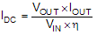
where
- VOUT is the output voltage of the boost regulator.
- IOUT is the output current of the boost regulator.
- VIN is the input voltage of the boost regulator.
- η is the power conversion efficiency.
Calculate the inductor current peak-to-peak ripple as in Equation 7.
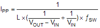
where
- IPP is the inductor peak-to-peak ripple.
- L is the inductor value.
- ƒSW is the switching frequency.
- VOUT is the output voltage.
- VIN is the input voltage.
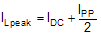
Therefore, the peak current, ILpeak, seen by the inductor is calculated with Equation 8.
With ISEL pin logic high, the peak switching current limit is 4.5A(typ), when the ISEL pin logic low, the peak switching current limit will change from 4.5A(typ) to 2.5A(typ). It is important that the peak current does not exceed the inductor saturation current.
For a given physical inductor size, increasing inductance usually results in an inductor with lower saturation current. The total losses of the coil consists of the DC resistance (DCR) loss and the following frequency-dependent loss:
- The losses in the core material (magnetic hysteresis loss, especially at high switching frequencies)
- Additional losses in the conductor from the skin effect (current displacement at high frequencies)
- Magnetic field losses of the neighboring windings (proximity effect)
For a certain inductor, the larger current ripple (smaller inductor) generates the higher DC and also the frequency-dependent loss. Usually, a data sheet of an inductor does not provide the core loss information. If needed, consult the inductor vendor for detailed information. An inductor with lower DCR is basically recommended for higher efficiency. However, it is usually a tradeoff between the loss and foot print. The table below lists some recommended inductors.
| PART NUMBER | L (μH) | DCR TYP (mΩ) | SATURATION CURRENT (A) | SIZE (L × W × H mm) | VENDOR(1) |
|---|---|---|---|---|---|
| XGL5050-222ME | 2.2 | 6.8 | 10.7 | 5.28 x 5.48 x 5.1 | Coilcraft |
| XGL5050-472ME | 4.7 | 13.9 | 7.0 | 5.28 x 5.48 x 5.1 | Coilcraft |
| XGL6060-103ME | 10 | 18.5 | 7.3 | 6.51 x 6.71 x 6.1 | Coilcraft |
| XGL4020-222ME | 2.2 | 19.5 | 6.2 | 4.0 x 4.0 x 2.1 | Coilcraft |
| XGL4020-472ME | 4.7 | 43 | 4.1 | 4.0 x 4.0 x 2.1 | Coilcraft |
| XGL4020-822ME | 8.2 | 71 | 3.2 | 4.0 x 4.0 x 2.1 | Coilcraft |