SLVSGQ1B January 2022 – January 2024 TPS61376
PRODUCTION DATA
- 1
- 1 Features
- 2 Applications
- 3 Description
- 4 Pin Configuration and Functions
- 5 Specifications
-
6 Detailed Description
- 6.1 Overview
- 6.2 Functional Block Diagram
- 6.3
Feature Description
- 6.3.1 VCC Power Supply
- 6.3.2 Enable and Programmable UVLO
- 6.3.3 Soft Start and Inrush Current Control During Start-Up
- 6.3.4 Switching Frequency
- 6.3.5 Adjustable input average Current Limit
- 6.3.6 Shut Down and Load Disconnect
- 6.3.7 Overvoltage Protection
- 6.3.8 Output Short Protection
- 6.3.9 Thermal Shutdown
- 6.4 Device Functional Modes
- 7 Application and Implementation
- 8 Device and Documentation Support
- 9 Revision History
- 10Mechanical, Packaging, and Orderable Information
Package Options
Mechanical Data (Package|Pins)
- RYH|13
Thermal pad, mechanical data (Package|Pins)
Orderable Information
7.4.2.1 Thermal Considerations
The maximum IC junction temperature should be restricted to 125°C under normal operating conditions. Calculate the maximum allowable dissipation, PD(max), and keep the actual power dissipation less than or equal to PD(max). The maximum-power-dissipation limit is determined using Equation 20.
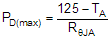
where
- TA is the maximum ambient temperature for the application.
- RθJA is the junction-to-ambient thermal resistance given in the Thermal Information table.
The TPS61376 comes in a thermally-enhanced VQFN package. The real junction-to-ambient thermal resistance of the package greatly depends on the PCB type, layout, and thermal pad connection. Using thick PCB copper and soldering the thermal pad to a large ground plate enhance the thermal performance. Using more vias connects the ground plate on the top layer and bottom layer around the IC without solder mask also improves the thermal capability.