SLVSFJ0B March 2021 – October 2021 TPS61379-Q1
PRODUCTION DATA
- 1 Features
- 2 Applications
- 3 Description
- 4 Revision History
- 5 Device Comparison Table
- 6 Pin Configuration and Functions
- 7 Specifications
-
8 Detailed Description
- 8.1 Overview
- 8.2 Functional Block Diagrams
- 8.3
Feature Description
- 8.3.1 VCC Power Supply
- 8.3.2 Input Undervoltage Lockout (UVLO)
- 8.3.3 Enable and Soft Start
- 8.3.4 Shut Down
- 8.3.5 Switching Frequency Setting
- 8.3.6 Spread Spectrum Frequency Modulation
- 8.3.7 Bootstrap
- 8.3.8 Load Disconnect
- 8.3.9 MODE/SYNC Configuration
- 8.3.10 Overvoltage Protection (OVP)
- 8.3.11 Output Short Protection/Hiccup
- 8.3.12 Power-Good Indicator
- 8.3.13 Thermal Shutdown
- 8.4 Device Functional Modes
-
9 Application and Implementation
- 9.1 Application Information
- 9.2
Typical Application
- 9.2.1 Design Requirements
- 9.2.2 Detailed Design Procedure
- 9.2.3 Application Curves
- 10Power Supply Recommendations
- 11Layout
- 12Device and Documentation Support
- 13Mechanical, Packaging, and Orderable Information
Package Options
Mechanical Data (Package|Pins)
- RTE|16
Thermal pad, mechanical data (Package|Pins)
- RTE|16
Orderable Information
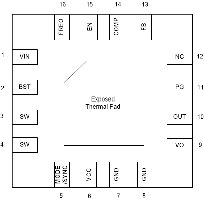
6 Pin Configuration and Functions
 Figure 6-1 16-Pin WQFN RTE Package (Transparent
Top View)
Figure 6-1 16-Pin WQFN RTE Package (Transparent
Top View)Table 6-1 Pin Functions
| PIN | I/O | DESCRIPTION | |
|---|---|---|---|
| NAME | NO. | ||
| VIN | 1 | I | IC power supply input |
| BST | 2 | I | Power supply for high-side N-MOSFET gate drivers. A capacitor must be connected between this pin and SW pin. |
| SW | 3, 4 | PWR | The switching node pin of the converter. It is connected to the drain of the internal low-side FET and the source of the high-side FET. |
| MODE/SYNC | 5 | I | Mode selection pin. MODE = high, forced PWM mode. MODE = low or floating, auto PFM mode. This pin can also be used to synchronize the external clock. Refer to Table 8-1 for details. |
| VCC | 6 | O | Output of internal regulator. A ceramic capacitor with more than 1 μF must be connected between this pin and GND. |
| GND | 7, 8 | PWR | Power ground of the IC. It is connected to the source of the low-side FET. |
| VO | 9 | PWR | Output of the isolation FET. Connect load to this pin to achieve input/output isolation. |
| OUT | 10 | PWR | Output of the drain of the HS FET. Connect this pin as the output can disable the load disconnect/short protection feature (or short this pin with VO pin). |
| PG | 11 | O | Power good indicator, open-drain output |
| NC | 12 | I | No connection pin |
| FB | 13 | I | Feedback pin. Use a resistor divider to set the desired output voltage. Refer to Section 9.2.2.1 for details. |
| COMP | 14 | I | Output of the internal transconductance error amplifier. An external RC network is connected to this pin to optimize the loop stability and response time. |
| EN | 15 | I | Enable logic input |
| FREQ | 16 | I | Frequency setting pin. Connect a resistor between this pin and GND pin to set the desired frequency. |
| Thermal Pad | - | - | The thermal pad must be connected to power ground plane for good power dissipation. |