SLVS833E March 2010 – October 2020 TPS62065 , TPS62067
PRODUCTION DATA
- 1 Features
- 2 Applications
- 3 Description
- 4 Revision History
- 5 Device Comparison Table
- 6 Pin Configuration and Functions
- 7 Specifications
- 8 Detailed Description
- 9 Application and Implementation
- 10Power Supply Recommendations
- 11Layout
- 12Device and Documentation Support
- 13Mechanical, Packaging, and Orderable Information
Package Options
Mechanical Data (Package|Pins)
- DSG|8
Thermal pad, mechanical data (Package|Pins)
- DSG|8
Orderable Information
9.2.2.1 Output Voltage Setting
The output voltage can be calculated to:
Equation 2. 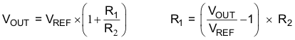
with an internal reference voltage VREF typically 0.6 V.
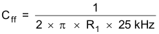
To minimize the current through the feedback divider network, R2 should be within the range of 120 kΩ to 360 kΩ. The sum of R1 and R2 should not exceed approximately 1 MΩ, to keep the network robust against noise. An external feed-forward capacitor Cff is required for optimum regulation performance. Lower resistor values can be used. R1 and Cff places a zero in the loop. The right value for Cff can be calculated as:
Equation 3. 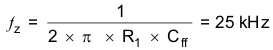
Equation 4.