SLVS833E March 2010 – October 2020 TPS62065 , TPS62067
PRODUCTION DATA
- 1 Features
- 2 Applications
- 3 Description
- 4 Revision History
- 5 Device Comparison Table
- 6 Pin Configuration and Functions
- 7 Specifications
- 8 Detailed Description
- 9 Application and Implementation
- 10Power Supply Recommendations
- 11Layout
- 12Device and Documentation Support
- 13Mechanical, Packaging, and Orderable Information
Package Options
Mechanical Data (Package|Pins)
- DSG|8
Thermal pad, mechanical data (Package|Pins)
- DSG|8
Orderable Information
9.2.2.2.1 Inductor Selection
The inductor value has a direct effect on the ripple current. The selected inductor must be rated for its DC resistance and saturation current. The inductor ripple current (ΔIL) decreases with higher inductance and increases with higher VIN or VOUT.
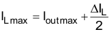
Equation 6 calculates the maximum inductor current in PWM mode under static load conditions. The saturation current of the inductor should be rated higher than the maximum inductor current as calculated with Equation 7. This is recommended because during heavy load transient the inductor current rises above the calculated value.
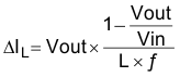
where
- f = Switching frequency (3 MHz typical)
- L = Inductor value
- ΔIL = Peak-to-peak inductor ripple current
- ILmax = Maximum inductor current
A more conservative approach is to select the inductor current rating just for the switch current limit ILIMF of the converter.
The total losses of the coil have a strong impact on the efficiency of the DC/DC conversion and consist of both the losses in the DC resistance R(DC) and the following frequency-dependent components:
- The losses in the core material (magnetic hysteresis loss, especially at high switching frequencies)
- Additional losses in the conductor from the skin effect (current displacement at high frequencies)
- Magnetic field losses of the neighboring windings (proximity effect)
- Radiation losses
| DIMENSIONS (mm3) | INDUCTANCE (μH) | INDUCTOR TYPE | SUPPLIER |
|---|---|---|---|
| 3.2 × 2.5 × 1 maximum | 1 | LQM32PN (MLCC) | Murata |
| 3.7 × 4 × 1.8 maximum | 1 | LQH44 (wire wound) | Murata |
| 4 × 4 × 2.6 maximum | 1.2 | NRG4026T (wire wound) | Taiyo Yuden |
| 3.5 × 3.7 × 1.8 maximum | 1.2 | DE3518 (wire wound) | TOKO |