SLVSB70C October 2013 – January 2021 TPS62085 , TPS62086 , TPS62087
PRODUCTION DATA
- 1 Features
- 2 Applications
- 3 Description
- 4 Revision History
- 5 Device Options
- 6 Pin Configuration and Functions
- 7 Specifications
- 8 Detailed Description
- 9 Application and Implementation
- 10Power Supply Recommendations
- 11Layout
- 12Device and Documentation Support
Package Options
Mechanical Data (Package|Pins)
- RLT|7
Thermal pad, mechanical data (Package|Pins)
Orderable Information
3 Description
The TPS62085, TPS62086, and TPS62087
devices are high-frequency synchronous step-down converters optimized for small
solution size and high efficiency. With an input voltage range of 2.5 V to
6.0 V, common battery technologies are supported. The
devices focus on high-efficiency step-down conversion over a wide output current
range. At medium to heavy loads, the converter operates in PWM mode and
automatically enters Power Save Mode operation at light load to maintain high
efficiency over the entire load current range.
To address the requirements of system power rails, the internal compensation circuit allows a large selection of external output capacitor values ranging from 10 µF to 150 µF. Together with its DCS-Control architecture, excellent load transient performance and output voltage regulation accuracy are achieved. The devices are available in a 2-mm × 2-mm VSON package.
| PART NUMBER | PACKAGE(1) | BODY SIZE (NOM) |
|---|---|---|
| TPS62085 | VSON (7) | 2.00 mm × 2.00 mm |
| TPS62086 | ||
| TPS62087 |
 Typical Application
Schematic
 Typical Application
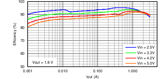
Efficiency