SLVSD94E November 2017 – November 2021 TPS62088 , TPS62088A , TPS62089A
PRODUCTION DATA
- 1 Features
- 2 Applications
- 3 Description
- 4 Revision History
- 5 Device Options
- 6 Pin Configuration and Functions
- 7 Specifications
- 8 Detailed Description
- 9 Application and Implementation
- 10Power Supply Recommendations
- 11Layout
- 12Device and Documentation Support
- 13Mechanical, Packaging, and Orderable Information
Package Options
Refer to the PDF data sheet for device specific package drawings
Mechanical Data (Package|Pins)
- YWC|6
- YFP|6
Thermal pad, mechanical data (Package|Pins)
Orderable Information
9.2.2.5 Inductor Selection
The main parameter for the inductor selection is the inductor value and then the saturation current of the inductor. To calculate the maximum inductor current under static load conditions, Equation 5 is given.
Equation 5. 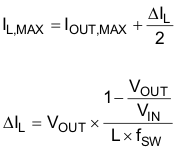
where
- IOUT,MAX = Maximum output current
- ΔIL = Inductor current ripple
- fSW = Switching frequency
- L = Inductor value
It is recommended to choose a saturation current for the inductor that is approximately 20% to 30% higher than IL,MAX. In addition, DC resistance and size should also be taken into account when selecting an appropriate inductor. Table 9-5 lists recommended inductors.
Table 9-5 List of Recommended Inductors(1)
| INDUCTANCE [µH] | CURRENT RATING [A] | DIMENSIONS [L × W × H mm] | DC RESISTANCE [mΩ] | PART NUMBER |
|---|---|---|---|---|
| 0.24 | 4.9 | 1.6 × 0.8 × 1.0 | 30 | Murata, DFE160810S-R24M (DFE18SANR24MG0) |
| 0.24 | 6.5 | 2.0 × 1.2 × 1.0 | 25 | Murata, DFE201210U-R24M |
| 0.24 | 4.9 | 1.6 × 0.8 × 0.8 | 22 | Cyntec, HTEH16080H-R24MSR |
| 0.25 | 9.7 | 4.0 × 4.0 × 1.2 | 7.64 | Coilcraft, XFL4012-251ME |
| 0.24 | 3.5 | 2.0 × 1.6 × 0.6 | 35 | Wurth Electronics, 74479977124 |
| 0.24 | 3.5 | 2.0 × 1.6 × 0.6 | 35 | Sunlord, MPM201606SR24M |
(1) See Third-party Products disclaimer.