SLVSD94E November   2017  – November 2021 TPS62088 , TPS62088A , TPS62089A

PRODUCTION DATA  

  1. Features
  2. Applications
  3. Description
  4. Revision History
  5. Device Options
  6. Pin Configuration and Functions
  7. Specifications
    1. 7.1 Absolute Maximum Ratings 
    2. 7.2 ESD Ratings
    3. 7.3 Recommended Operating Conditions
    4. 7.4 Thermal Information 
    5. 7.5 Electrical Characteristics
    6. 7.6 Typical Characteristics
  8. Detailed Description
    1. 8.1 Overview
    2. 8.2 Functional Block Diagram
    3. 8.3 Feature Description
      1. 8.3.1 Power Save Mode
      2. 8.3.2 Pulse Width Modulation (PWM) Operation
      3. 8.3.3 100% Duty Cycle Low Dropout Operation
      4. 8.3.4 Soft Start
      5. 8.3.5 Switch Current Limit and HICCUP Short-Circuit Protection
      6. 8.3.6 Undervoltage Lockout
      7. 8.3.7 Thermal Shutdown
    4. 8.4 Device Functional Modes
      1. 8.4.1 Enable and Disable
      2. 8.4.2 Power Good
  9. Application and Implementation
    1. 9.1 Application Information
    2. 9.2 Typical Application
      1. 9.2.1 Design Requirements
      2. 9.2.2 Detailed Design Procedure
        1. 9.2.2.1 Custom Design With WEBENCH® Tools
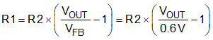
        2. 9.2.2.2 Setting The Output Voltage
        3. 9.2.2.3 Feedforward Capacitor
        4. 9.2.2.4 Output Filter Design
        5. 9.2.2.5 Inductor Selection
        6. 9.2.2.6 Capacitor Selection
      3. 9.2.3 Application Curves
  10. 10Power Supply Recommendations
  11. 11Layout
    1. 11.1 Layout Guidelines
    2. 11.2 Layout Example
      1. 11.2.1 Thermal Considerations
  12. 12Device and Documentation Support
    1. 12.1 Device Support
      1. 12.1.1 Third-Party Products Disclaimer
      2. 12.1.2 Development Support
        1. 12.1.2.1 Custom Design With WEBENCH® Tools
    2. 12.2 Documentation Support
      1. 12.2.1 Related Documentation
    3. 12.3 Receiving Notification of Documentation Updates
    4. 12.4 Support Resources
    5. 12.5 Trademarks
    6. 12.6 Electrostatic Discharge Caution
    7. 12.7 Glossary
  13. 13Mechanical, Packaging, and Orderable Information

Package Options

Refer to the PDF data sheet for device specific package drawings

Mechanical Data (Package|Pins)
  • YFP|6
Thermal pad, mechanical data (Package|Pins)
Orderable Information

Setting The Output Voltage

Choose resistors R1 and R2 to set the output voltage within a range of 0.6V to 4V, according to Equation 3. To keep the feedback (FB) net robust from noise, set R2 equal to or lower than 100 kΩ to have at least 0.6 µA of current in the voltage divider. Lower values of FB resistors achieve better noise immunity, and lower light load efficiency, as explained in the Design Considerations For A Resistive Feedback Divider In A DC/DC Converter Analog Design Journal.

Equation 3. GUID-E9090B62-03B3-4704-9703-C292C40625D7-low.gif

For devices with a fixed output voltage, the FB pin must be connected to VOUT. R1, R2, and C4 are not needed. The fixed output voltage devices have an internal feedforward capacitor.