SLVSC55C August 2013 – November 2021 TPS62090-Q1
PRODUCTION DATA
- 1 Features
- 2 Applications
- 3 Description
- 4 Revision History
- 5 Pin Configuration and Functions
- 6 Specifications
-
7 Detailed Description
- 7.1 Overview
- 7.2 Functional Block Diagram
- 7.3
Feature Description
- 7.3.1 Enable and Disable (EN)
- 7.3.2 Soft Start (SS) and Hiccup Current Limit During Start-Up
- 7.3.3 Voltage Tracking (SS)
- 7.3.4 Short-Circuit Protection (Hiccup Mode)
- 7.3.5 Output Discharge Function
- 7.3.6 Power Good Output (PG)
- 7.3.7 Frequency Set Pin (FREQ)
- 7.3.8 Undervoltage Lockout (UVLO)
- 7.3.9 Thermal Shutdown
- 7.3.10 Charge Pump (CP, CN)
- 7.4 Device Functional Modes
- 8 Application and Implementation
- 9 Power Supply Recommendations
- 10Layout
- 11Device and Documentation Support
- 12Mechanical, Packaging, and Orderable Information
Package Options
Mechanical Data (Package|Pins)
- RGT|16
Thermal pad, mechanical data (Package|Pins)
- RGT|16
Orderable Information
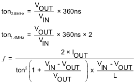
7.4.2 Power Save Mode Operation
As the load current decreases, the converter enters power save mode operation. During power save mode, the converter operates with reduced switching frequency in PFM mode and with a minimum quiescent current while maintaining high efficiency. The power save mode is based on a fixed on-time architecture following Equation 3. When operating at 1.4 MHz, the on-time is twice as long as the on-time for 2.8-MHz operation, resulting in larger output voltage ripple, as shown in Figure 8-11 and Figure 8-12, and slightly higher output voltage at no load, as shown in Figure 8-8 and Figure 8-9. To have the same output voltage ripple at 1.4 MHz during PFM mode, either the output capacitor or the inductor value must be increased. As an example, operating at 2.8 MHz using
0.47-µH inductor gives the same output voltage ripple as operating with 1.4 MHz using 1-µH inductor.
In power save mode the output voltage rises slightly above the nominal output voltage in PWM mode, as shown in Figure 8-8 and Figure 8-9. This effect is reduced by increasing the output capacitance or the inductor value. This effect is also reduced by programming the output voltage of the TPS62090Q lower than the target value. As an example, if the target output voltage is 3.3 V, then the TPS62090Q is programmed to 3.3 V – 0.8%. As a result the output voltage accuracy is now –2.2% to +2.2% instead of –1.4% to 3%. The output voltage accuracy in PFM operation is reflected in the Section 6.5 table and given for a 22-µF output capacitance.