SLVSC55C August 2013 – November 2021 TPS62090-Q1
PRODUCTION DATA
- 1 Features
- 2 Applications
- 3 Description
- 4 Revision History
- 5 Pin Configuration and Functions
- 6 Specifications
-
7 Detailed Description
- 7.1 Overview
- 7.2 Functional Block Diagram
- 7.3
Feature Description
- 7.3.1 Enable and Disable (EN)
- 7.3.2 Soft Start (SS) and Hiccup Current Limit During Start-Up
- 7.3.3 Voltage Tracking (SS)
- 7.3.4 Short-Circuit Protection (Hiccup Mode)
- 7.3.5 Output Discharge Function
- 7.3.6 Power Good Output (PG)
- 7.3.7 Frequency Set Pin (FREQ)
- 7.3.8 Undervoltage Lockout (UVLO)
- 7.3.9 Thermal Shutdown
- 7.3.10 Charge Pump (CP, CN)
- 7.4 Device Functional Modes
- 8 Application and Implementation
- 9 Power Supply Recommendations
- 10Layout
- 11Device and Documentation Support
- 12Mechanical, Packaging, and Orderable Information
Package Options
Mechanical Data (Package|Pins)
- RGT|16
Thermal pad, mechanical data (Package|Pins)
- RGT|16
Orderable Information
8.2.2.1 Inductor Selection
The inductor selection is affected by several parameters such as inductor-ripple current, output-voltage ripple, transition point into power save mode, and efficiency. See Table 8-4 for typical inductors.
| INDUCTOR VALUE | COMPONENT SUPPLIER | SIZE (L × W × H mm) | Isat / DCR |
|---|---|---|---|
| 0.6 µH | Coilcraft XAL4012-601 | 4 × 4 × 2.1 | 7.1 A / 9.5 mΩ |
| 1 µH | Coilcraft XAL4020-102 | 4 × 4 × 2.1 | 5.9 A / 13.2 mΩ |
| 1 µH | Coilcraft XFL4020-102 | 4 × 4 × 2.1 | 5.1 A / 10.8 mΩ |
| 0.47 µH | TOKO DFE252012 R47 | 2.5 × 2 × 1.2 | 3.7 A / 39 mΩ |
| 1 µH | TOKO DFE252012 1R0 | 2.5 × 2 × 1.2 | 3.0 A / 59 mΩ |
| 0.68 µH | TOKO DFE322512 R68 | 3.2 × 2.5 × 1.2 | 3.5 A / 37 mΩ |
| 1 µH | TOKO DFE322512 1R0 | 3.2 × 2.5 × 1.2 | 3.1 A / 45 mΩ |
In addition, the inductor must be rated for the appropriate saturation current and DC resistance (DCR). The inductor must be rated for a saturation current as high as the typical switch current limit, of 4.6 A or according to Equation 5 and Equation 6. Equation 5 and Equation 6 calculate the maximum inductor current under static load conditions. The formula takes the converter efficiency into account. The converter efficiency is taken from the Section 6.6 graphs or 80% can be used as a conservative approach. The calculation must be done for the maximum input voltage where the peak switch current is highest.
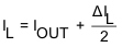
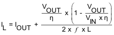
where
- ƒ = Converter switching frequency (typical 2.8 MHz or 1.4 MHz)
- L = Selected inductor value
- η = Estimated converter efficiency (use the number from the efficiency curves or 0.80 as an conservative assumption)
The calculation must be done for the maximum input voltage of the application
Calculating the maximum inductor current using the actual operating conditions gives the minimum saturation current. A margin of 20% must be added to cover for load transients during operation.