SLVSCD6A December   2015  – January 2021 TPS62097

PRODUCTION DATA  

  1. Features
  2. Applications
  3. Description
  4. Revision History
  5. Device Options
  6. Pin Configuration and Functions
  7. Specifications
    1. 7.1 Absolute Maximum Ratings
    2. 7.2 ESD Ratings
    3. 7.3 Recommend Operating Conditions
    4. 7.4 Thermal Information
    5. 7.5 Electrical Characteristics
    6. 7.6 Typical Characteristics
  8. Detailed Description
    1. 8.1 Overview
    2. 8.2 Functional Block Diagram
    3. 8.3 Feature Description
      1. 8.3.1 100% Duty Cycle Mode
      2. 8.3.2 Switch Current Limit and Hiccup Short Circuit Protection
      3. 8.3.3 Undervoltage Lockout (UVLO)
      4. 8.3.4 Thermal Shutdown
    4. 8.4 Device Function Modes
      1. 8.4.1 Enable and Disable (EN)
      2. 8.4.2 Power Save Mode and Forced PWM Mode (MODE)
      3. 8.4.3 Soft Start-up (SS/TR)
      4. 8.4.4 Voltage Tracking (SS/TR)
      5. 8.4.5 Power Good (PG)
  9. Application and Implementation
    1. 9.1 Application Information
    2. 9.2 1.2-V Output Application
      1. 9.2.1 Design Requirements
      2. 9.2.2 Detailed Design Procedure
        1. 9.2.2.1 Setting the Output Voltage
        2. 9.2.2.2 Output Filter Design
        3. 9.2.2.3 Inductor Selection
        4. 9.2.2.4 Capacitor Selection
      3. 9.2.3 Application Performance Curves
      4. 9.2.4 Coincidental Voltage Tracking
        1. 9.2.4.1 Design Requirements
        2. 9.2.4.2 Detailed Design Procedure
        3. 9.2.4.3 Application Performance Curve
      5. 9.2.5 Switching Frequency Selection
        1. 9.2.5.1 Design Requirements
        2. 9.2.5.2 Detailed Design Procedure
        3. 9.2.5.3 Application Performance Curves
  10. 10Power Supply Recommendations
  11. 11Layout
    1. 11.1 Layout Guidelines
    2. 11.2 Layout Example
      1. 11.2.1 Thermal Information
  12. 12Device and Documentation Support
    1. 12.1 Device Support
      1. 12.1.1 Third-Party Products Disclaimer
    2. 12.2 Support Resources
    3. 12.3 Receiving Notification of Documentation Updates
    4. 12.4 Trademarks
    5. 12.5 Electrostatic Discharge Caution
    6. 12.6 Glossary
  13. 13Mechanical, Packaging, and Orderable Information

Package Options

Mechanical Data (Package|Pins)
Thermal pad, mechanical data (Package|Pins)
Orderable Information

Setting the Output Voltage

The output voltage is set by an external resistor divider according to Equation 4:

Equation 4. GUID-CDB7607C-D522-46EC-A738-61FEF8339C89-low.gif

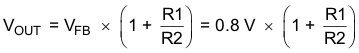
R2 should not be higher than 20 kΩ to reduce noise coupling into the FB pin and improve the output voltage regulation. Figure 9-1 shows the external resistor divider value for 1.2-V output. Choose additional resistor values for other outputs. A feedforward capacitor is not required.

The fixed output voltage versions, TPS6209718 and TPS6209733, do not need the external resistor divider. TI recommends to connect the FB pin to AGND for improved thermal performance.