SLVSCD6A December 2015 – January 2021 TPS62097
PRODUCTION DATA
- 1 Features
- 2 Applications
- 3 Description
- 4 Revision History
- 5 Device Options
- 6 Pin Configuration and Functions
- 7 Specifications
- 8 Detailed Description
- 9 Application and Implementation
- 10Power Supply Recommendations
- 11Layout
- 12Device and Documentation Support
- 13Mechanical, Packaging, and Orderable Information
Package Options
Mechanical Data (Package|Pins)
- RWK|11
Thermal pad, mechanical data (Package|Pins)
Orderable Information
8.4.2 Power Save Mode and Forced PWM Mode (MODE)
The MODE pin is a multi-functional pin that allows the device operation in forced PWM mode or PWM/PSM mode, and to select the PWM switching frequency.
Once the EN pin is pulled high, the IC enables internal circuit blocks and prepares to ramp the output up. The period between the rising edge of the EN pin and the beginning of the power stage switching is called the MODE detection time, typically 50 µs. During the MODE detection time period, shown in Figure 8-1, the PWM switching frequency and operating mode are set by the MODE pin status, as shown in Table 8-1.
The PWM switching frequency cannot be changed after the detection time period. Only when the device is set in PWM/PSM mode during the MODE detection time period (MODE = AGND), it is possible to switch between PWM/PSM and forced PWM operation modes by toggling the MODE pin with a GPIO pin of a microcontroller, for example. The other four MODE pin selections force the device in PWM mode only.
 Figure 8-1 Power-up Sequence
| TYPICAL PWM SWITCHING FREQUENCY (MHZ) | RESISTANCE AT MODE PIN (E24 EIA VALUE) | TOGGLE MODE PIN AFTER MODE DETECTION | ON-TIME EQUATION | OPERATING MODE |
|---|---|---|---|---|
| 1.50 | 8.2 kΩ ±5% | No | tON = 667 ns x VOUT / VIN | Forced PWM |
| 1.75 | 18 kΩ ±5% | No | tON = 571 ns x VOUT / VIN | Forced PWM |
| 2.00 | AGND | Yes | tON = 500 ns x VOUT / VIN | PWM/PSM and Forced PWM |
| 2.25 | 39 kΩ ±5% | No | tON = 444 ns x VOUT / VIN | Forced PWM |
| 2.50 | 75 kΩ ±5% or Open | No | tON = 400 ns x VOUT / VIN | Forced PWM |
Connecting the MODE pin to AGND with a resistor or leaving the MODE pin open forces the device into PWM mode for the whole load range. The device operates with a fixed switching frequency that allows simple filtering of the switching frequency for noise sensitive applications. In forced PWM mode, the efficiency is lower than that of PSM at light load.
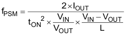
Connecting the MODE pin to the AGND pin enables Power Save Mode with an automatic transition between PWM and Power Save Mode. As the load current decreases and the inductor current becomes discontinuous, the device enters Power Save Mode operation automatically. In Power Save Mode, the switching frequency is reduced and estimated by Equation 2. In Power Save Mode, the output voltage rises slightly above the nominal output voltage, as shown in Figure 9-8. This effect is minimized by increasing the output capacitor.
When the device operates close to 100% duty cycle mode, the TPS62097 cannot enter Power Save Mode regardless of the load current if the input voltage decreases to typically 15% above the output voltage. The device maintains output regulation in PWM mode.