SLVSAG7F November   2011  – November 2021 TPS62130 , TPS62130A , TPS62131 , TPS62132 , TPS62133

PRODUCTION DATA  

  1. Features
  2. Applications
  3. Description
  4. Revision History
  5. Device Comparison Table
  6. Pin Configuration and Functions
  7. Specifications
    1. 7.1 Absolute Maximum Ratings (1)
    2. 7.2 ESD Ratings
    3. 7.3 Recommended Operating Conditions
    4. 7.4 Thermal Information
    5. 7.5 Electrical Characteristics
    6. 7.6 Typical Characteristics
  8. Detailed Description
    1. 8.1 Overview
    2. 8.2 Functional Block Diagram
    3. 8.3 Feature Description
      1. 8.3.1 Enable / Shutdown (EN)
      2. 8.3.2 Soft Start / Tracking (SS/TR)
      3. 8.3.3 Power Good (PG)
      4. 8.3.4 Pin-Selectable Output Voltage (DEF)
      5. 8.3.5 Frequency Selection (FSW)
      6. 8.3.6 Undervoltage Lockout (UVLO)
      7. 8.3.7 Thermal Shutdown
    4. 8.4 Device Functional Modes
      1. 8.4.1 Pulse Width Modulation (PWM) Operation
      2. 8.4.2 Power Save Mode Operation
      3. 8.4.3 100% Duty-Cycle Operation
      4. 8.4.4 Current Limit And Short Circuit Protection
  9. Application and Implementation
    1. 9.1 Application Information
    2. 9.2 Typical Application
      1. 9.2.1 Design Requirements
      2. 9.2.2 Detailed Design Procedure
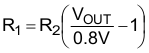
        1. 9.2.2.1 Programming The Output Voltage
        2. 9.2.2.2 External Component Selection
          1. 9.2.2.2.1 Inductor Selection
          2. 9.2.2.2.2 Capacitor Selection
            1. 9.2.2.2.2.1 Output Capacitor
            2. 9.2.2.2.2.2 Input Capacitor
            3. 9.2.2.2.2.3 Soft-Start Capacitor
        3. 9.2.2.3 Tracking Function
        4. 9.2.2.4 Output Filter And Loop Stability
      3. 9.2.3 Application Curves
    3. 9.3 System Examples
      1. 9.3.1 LED Power Supply
      2. 9.3.2 Active Output Discharge
      3. 9.3.3 –3.3-V Inverting Power Supply
      4. 9.3.4 Various Output Voltages
  10. 10Power Supply Recommendations
  11. 11Layout
    1. 11.1 Layout Guidelines
    2. 11.2 Layout Example
    3. 11.3 Thermal Information
  12. 12Device and Documentation Support
    1. 12.1 Device Support
      1. 12.1.1 Third-Party Products Disclaimer
    2. 12.2 Documentation Support
      1. 12.2.1 Related Documentation
    3. 12.3 Receiving Notification of Documentation Updates
    4. 12.4 Support Resources
    5. 12.5 Trademarks
    6. 12.6 Electrostatic Discharge Caution
    7. 12.7 Glossary
  13. 13Mechanical, Packaging, and Orderable Information

Package Options

Mechanical Data (Package|Pins)
Thermal pad, mechanical data (Package|Pins)
Orderable Information

Programming The Output Voltage

While the output voltage of the TPS62130 (TPS62130A) is adjustable, the TPS62131, TPS62132, and TPS62133 are programmed to fixed output voltages. For fixed output voltage versions, the FB pin is pulled down internally and can be left floating. It is recommended to connect to AGND to improve thermal resistance. The adjustable version can be programmed for output voltages from 0.9 V to 6 V by using a resistive divider from VOUT to AGND. The voltage at the FB pin is regulated to 800 mV. The value of the output voltage is set by the selection of the resistive divider from Equation 6. It is recommended to choose resistor values that allow a current of at least 2 μA, meaning the value of R2 should not exceed 400 kΩ. Lower resistor values are recommended for the highest accuracy and most robust design. For applications requiring lowest current consumption, the use of fixed output voltage versions is recommended.

Equation 6. GUID-B9D0DDC4-E0B9-4A05-9BA3-E2CC77B37950-low.gif

In case the FB pin gets opened, the device clamps the output voltage at the VOS pin internally to approximately 7.4 V.