SLVSAL5E November   2011  – October 2021 TPS62150 , TPS62150A , TPS62151 , TPS62152 , TPS62153

PRODUCTION DATA  

  1. Features
  2. Applications
  3. Description
  4. Revision History
  5. Device Comparison Table
  6. Pin Configuration and Functions
  7. Specifications
    1. 7.1 Absolute Maximum Ratings (1)
    2. 7.2 ESD Ratings
    3. 7.3 Recommended Operating Conditions
    4. 7.4 Thermal Information
    5. 7.5 Electrical Characteristics
    6. 7.6 Typical Characteristics
  8. Detailed Description
    1. 8.1 Overview
    2. 8.2 Functional Block Diagrams
    3. 8.3 Feature Description
      1. 8.3.1 Enable / Shutdown (EN)
      2. 8.3.2 Soft Start or Tracking (SS/TR)
      3. 8.3.3 Power Good (PG)
      4. 8.3.4 Pin-Selectable Output Voltage (DEF)
      5. 8.3.5 Frequency Selection (FSW)
      6. 8.3.6 Undervoltage Lockout (UVLO)
      7. 8.3.7 Thermal Shutdown
    4. 8.4 Device Functional Modes
      1. 8.4.1 Pulse-Width Modulation (PWM) Operation
      2. 8.4.2 Power-Save Mode Operation
      3. 8.4.3 100% Duty-Cycle Operation
      4. 8.4.4 Current-Limit and Short-Circuit Protection
  9. Application and Implementation
    1. 9.1 Application Information
    2. 9.2 Typical Application
      1. 9.2.1 Design Requirements
      2. 9.2.2 Detailed Design Procedure
        1. 9.2.2.1 Programming the Output Voltage
        2. 9.2.2.2 External Component Selection
          1. 9.2.2.2.1 Inductor Selection
          2. 9.2.2.2.2 Capacitor Selection
            1. 9.2.2.2.2.1 Output Capacitor
            2. 9.2.2.2.2.2 Input Capacitor
            3. 9.2.2.2.2.3 Soft-Start Capacitor
        3. 9.2.2.3 Tracking Function
        4. 9.2.2.4 Output Filter and Loop Stability
      3. 9.2.3 Application Curves
    3. 9.3 System Examples
      1. 9.3.1 LED Power Supply
      2. 9.3.2 Active Output Discharge
      3. 9.3.3 Inverting Power Supply
      4. 9.3.4 Various Output Voltages
  10. 10Power Supply Recommendations
  11. 11Layout
    1. 11.1 Layout Guidelines
    2. 11.2 Layout Example
      1. 11.2.1 Thermal Considerations
  12. 12Device and Documentation Support
    1. 12.1 Device Support
      1. 12.1.1 Third-Party Products Disclaimer
    2. 12.2 Documentation Support
      1. 12.2.1 Related Documentation
    3. 12.3 Receiving Notification of Documentation Updates
    4. 12.4 Support Resources
    5. 12.5 Trademarks
    6. 12.6 Electrostatic Discharge Caution
    7. 12.7 Glossary
  13. 13Mechanical, Packaging, and Orderable Information

Package Options

Mechanical Data (Package|Pins)
Thermal pad, mechanical data (Package|Pins)
Orderable Information

Current-Limit and Short-Circuit Protection

The TPS6215x devices have protection against heavy-load and short-circuit events. At heavy loads, the current limit determines the maximum output current. If the current limit is reached, the high-side FET is turned off. Avoiding shoot-through current, then the low-side FET switches on to allow the inductor current to decrease. The low-side current limit is typically 1.2 A. The high-side FET turns on again only if the current in the low-side FET has decreased below the low-side current-limit threshold.

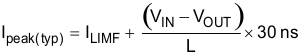
The output current of the device is limited by the current limit (see Section 7.5). Due to internal propagation delay, the actual current can exceed the static current limit during that time. The dynamic current limit is calculated as follows:
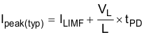
Equation 4. GUID-62020CE5-420C-415F-8A09-8EF58DC23696-low.gif

where

  • ILIMF is the static current limit, specified in the Section 7.5
  • VL is the voltage across the inductor (VIN – VOUT)
  • L is the inductor value
  • tPD is the internal propagation delay

The current limit can exceed static values, especially if the input voltage is high and the application uses very small inductances. Calculate the peak current in the dynamic high-side switch using the following equation:

Equation 5. GUID-BADE82C2-6B7F-42A6-AA48-7DBCE17CC7E8-low.gif