SLVSAM2E November   2011  – May 2017 TPS62160 , TPS62161 , TPS62162 , TPS62163

PRODUCTION DATA.  

  1. Features
  2. Applications
  3. Description
  4. Revision History
  5. Device Voltage Options
  6. Pin Configuration and Functions
  7. Specifications
    1. 7.1 Absolute Maximum Ratings
    2. 7.2 ESD Ratings
    3. 7.3 Recommended Operating Conditions
    4. 7.4 Thermal Information
    5. 7.5 Electrical Characteristics
    6. 7.6 Typical Characteristics
  8. Detailed Description
    1. 8.1 Overview
    2. 8.2 Functional Block Diagrams
    3. 8.3 Feature Description
      1. 8.3.1 Enable and Shutdown (EN)
      2. 8.3.2 Current Limit and Short Circuit Protection
      3. 8.3.3 Power Good (PG)
      4. 8.3.4 Undervoltage Lockout (UVLO)
      5. 8.3.5 Thermal Shutdown
    4. 8.4 Device Functional Modes
      1. 8.4.1 Soft Start
      2. 8.4.2 Pulse Width Modulation (PWM) Operation
      3. 8.4.3 Power Save Mode Operation
      4. 8.4.4 100% Duty-Cycle Operation
  9. Application and Implementation
    1. 9.1 Application Information
    2. 9.2 Typical Application
      1. 9.2.1 Design Requirements
      2. 9.2.2 Detailed Design Procedure
        1. 9.2.2.1 Custom Design with WEBENCH® Tools
        2. 9.2.2.2 Programming the Output Voltage
        3. 9.2.2.3 External Component Selection
        4. 9.2.2.4 Inductor Selection
        5. 9.2.2.5 Capacitor Selection
          1. 9.2.2.5.1 Output Capacitor
          2. 9.2.2.5.2 Input Capacitor
        6. 9.2.2.6 Output Filter and Loop Stability
        7. 9.2.2.7 TPS6216x Components List
      3. 9.2.3 Application Curves
    3. 9.3 System Examples
      1. 9.3.1 1-A Power Supply
      2. 9.3.2 Inverting Power Supply
  10. 10Power Supply Recommendations
  11. 11Layout
    1. 11.1 Layout Guidelines
    2. 11.2 Layout Example
    3. 11.3 Thermal Considerations
  12. 12Device and Documentation Support
    1. 12.1 Custom Design With WEBENCH® Tools
    2. 12.2 Device Support
      1. 12.2.1 Third-Party Products Disclaimer
    3. 12.3 Documentation Support
      1. 12.3.1 Related Documentation
    4. 12.4 Related Links
    5. 12.5 Community Resources
    6. 12.6 Trademarks
    7. 12.7 Electrostatic Discharge Caution
    8. 12.8 Glossary
  13. 13Mechanical, Packaging, and Orderable Information

Package Options

Mechanical Data (Package|Pins)
Thermal pad, mechanical data (Package|Pins)
Orderable Information

Pin Configuration and Functions

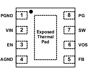
DSG Package
8-Pin WSON With Exposed Thermal Pad
Top View
TPS62160 TPS62161 TPS62162 TPS62163 SLVSAM2_pinout_DSG.gif
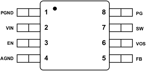
DGK Package
8-Pin VSSOP
Top View
TPS62160 TPS62161 TPS62162 TPS62163 SLVSAM2_pinout_DGK.gif
SPACE

Pin Functions

PIN(1) I/O DESCRIPTION
NAME NO.
PGND 1 Power ground
VIN 2 I Supply voltage
EN 3 I Enable input (High = enabled, Low = disabled)
AGND 4 Analog ground
FB 5 I Voltage feedback of adjustable version. Connect resistive voltage divider to this pin. It is recommended to connect FB to AGND on fixed output voltage versions for improved thermal performance.
VOS 6 I Output voltage sense pin and connection for the control loop circuitry.
SW 7 O Switch node, which is connected to the internal MOSFET switches. Connect inductor between SW and output capacitor.
PG 8 O Output power good (High = VOUT ready, Low = VOUT below nominal regulation); open drain (requires pull-up resistor; goes high impedance, when device is switched off)
Exposed Thermal Pad(2) Must be connected to AGND. Must be soldered to achieve appropriate power dissipation and mechanical reliability.
For more information about connecting pins, see Detailed Description and Application Information sections.
The exposed thermal pad is available with the DSG package only, not with DGK package.