SLUSDN9B November   2021  – July 2022 TPS62441-Q1 , TPS62442-Q1

PRODUCTION DATA  

  1. Features
  2. Applications
  3. Description
  4. Revision History
  5. Device Comparison Table
  6. Pin Configuration and Functions
  7. Specifications
    1. 7.1 Absolute Maximum Ratings
    2. 7.2 ESD Ratings
    3. 7.3 Recommended Operating Conditions
    4. 7.4 Thermal Information
    5. 7.5 Electrical Characteristics
    6. 7.6 Timing Requirements
    7. 7.7 Typical Characteristics
  8. Parameter Measurement Information
    1. 8.1 Schematic
  9. Detailed Description
    1. 9.1 Overview
    2. 9.2 Functional Block Diagram
    3. 9.3 Feature Description
      1. 9.3.1 Precise Enable (EN)
      2. 9.3.2 COMP/FSET
      3. 9.3.3 MODE/SYNC
      4. 9.3.4 Spread Spectrum Clocking (SSC)
      5. 9.3.5 Undervoltage Lockout (UVLO)
      6. 9.3.6 Power-Good Output (PG)
      7. 9.3.7 Thermal Shutdown
    4. 9.4 Device Functional Modes
      1. 9.4.1 Pulse Width Modulation (PWM) Operation
      2. 9.4.2 Power Save Mode Operation (PWM and PFM)
      3. 9.4.3 100% Duty-Cycle Operation
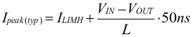
      4. 9.4.4 Current Limit and Short Circuit Protection
      5. 9.4.5 Foldback Current Limit and Short Circuit Protection
      6. 9.4.6 Output Discharge
      7. 9.4.7 Soft Start
  10. 10Application and Implementation
    1. 10.1 Application Information
      1. 10.1.1 Programming the Output Voltage
      2. 10.1.2 External Component Selection
        1. 10.1.2.1 Inductor Selection
        2. 10.1.2.2 Capacitor Selection
          1. 10.1.2.2.1 Input Capacitor
          2. 10.1.2.2.2 Output Capacitor
    2. 10.2 Typical Application
      1. 10.2.1 Design Requirements
      2. 10.2.2 Detailed Design Procedure
      3. 10.2.3 Application Curves
  11. 11Power Supply Recommendations
  12. 12Layout
    1. 12.1 Layout Guidelines
    2. 12.2 Layout Example
  13. 13Device and Documentation Support
    1. 13.1 Device Support
      1. 13.1.1 Third-Party Products Disclaimer
    2. 13.2 Documentation Support
      1. 13.2.1 Related Documentation
    3. 13.3 Receiving Notification of Documentation Updates
    4. 13.4 Support Resources
    5. 13.5 Trademarks
    6. 13.6 Electrostatic Discharge Caution
    7. 13.7 Glossary
  14. 14Mechanical, Packaging, and Orderable Information

Package Options

Mechanical Data (Package|Pins)
Thermal pad, mechanical data (Package|Pins)
Orderable Information

Current Limit and Short Circuit Protection

The TPS6244x-Q1 is protected against overload and short circuit events. The converter is not switching with the fixed frequency when in current limit. The converter resumes the fixed-frequency operation when the converter leaves current limit condition. If the inductor current exceeds the current limit, ILIMH, the high-side switch is turned off and the low-side switch is turned on to ramp down the inductor current. The high-side switch turns on again only if the current in the low-side switch has decreased below the low-side current limit, which can cause bursts or single pulses between the high-side and low-side current limit. Due to internal propagation delay, the actual current can exceed the static current limit. The dynamic current limit is given as:
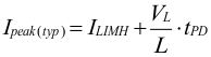
Equation 4. GUID-5B38BDCE-C1DD-4D2A-A992-5A24AE9ADD3F-low.gif

where

  • ILIMH is the static current limit as specified in the electrical characteristics.
  • L is the effective inductance at the peak current.
  • VL is the voltage across the inductor (VIN – VOUT).
  • tPD is the internal propagation delay of typically 50 ns.

The current limit can exceed static values, especially if the input voltage is high and very small inductances are used. The dynamic high-side switch peak current can be calculated as follows:

Equation 5. GUID-D292A9A7-2F33-4FAB-B20B-EB18C7A9D70A-low.gif