SLVS848D July 2009 – October 2015 TPS62620 , TPS62621 , TPS62622 , TPS62623 , TPS62624 , TPS62625
PRODUCTION DATA.
- 1 Features
- 2 Applications
- 3 Description
- 4 Revision History
- 5 Device Comparison Table
- 6 Pin Configuration and Functions
- 7 Specifications
- 8 Detailed Description
- 9 Application and Implementation
- 10Power Supply Recommendations
- 11Layout
- 12Device and Documentation Support
- 13Mechanical, Packaging, and Orderable Information
Package Options
Mechanical Data (Package|Pins)
- YFF|6
Thermal pad, mechanical data (Package|Pins)
Orderable Information
1 Features
- Wide Input Voltage Range from 2.3 V to 5.5 V
- 6 MHz Regulated Frequency Operation
- 90% Efficiency at 6 MHz Operation
- 31 μA Quiescent Current
- Best in Class Load and Line Transient
- ±2% Total DC Voltage Accuracy
- Automatic PFM/PWM Mode Switching
- Low Ripple Light-Load PFM Mode
- Internal Soft Start, 120-μs Start-Up Time
- Integrated Active Power-Down Sequencing (TPS62624 only)
- Current Overload and Thermal Shutdown Protection
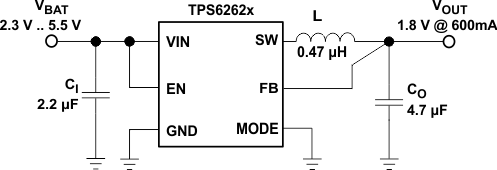
- Three Surface-Mount External Components Required (One MLCC Inductor, Two Ceramic Capacitors)
- Complete Sub 1-mm Component Profile Solution
- Total Solution Size < 12 mm2
- Available in a 6-Pin NanoFree™ (WCSP)
Regular and Ultra-Thin Packaging
2 Applications
- Mobile Phones, Smartphones
- WLAN, GPS and Bluetooth™ Applications
- DTV Tuner Applications
- DC/DC Micro Modules
spacer
3 Description
The TPS6262x device family provides high-frequency synchronous step-down DC/DC converters optimized for battery-powered portable applications. Intended for low-power applications, the TPS6262x devices support up to 600 mA load current, and allow the use of low cost chip inductor and capacitors.
With a wide input voltage range of 2.3 V to 5.5 V, the devices support applications powered by Li-Ion batteries with extended voltage range. Different fixed voltage output versions are available from 1.2 V to 2.3 V.
The TPS6262x devices operate at a regulated 6-MHz switching frequency and enter the power-save mode operation at light load currents to maintain high efficiency over the entire load current range.
The pulse frequency modulation (PFM) mode extends the battery life by reducing the quiescent current to 31 μA (typical) during light load and standby operation. For noise-sensitive applications, the device can be forced into fixed frequency pulse width modulation (PWM) mode by pulling the MODE pin high.
The TPS6262x devices operate over a free air temperature range of –40°C to 85°C. They are available in a 6-pin chip-scale package (WCSP).
Device Information(1)
| PART NUMBER | PACKAGE | BODY SIZE (NOM) |
|---|---|---|
| TPS6262x | DSBGA (6) | 1.30 mm × 0.96 mm |
- For all available packages, see the orderable addendum at the end of the datasheet.
Typical Application Schematic

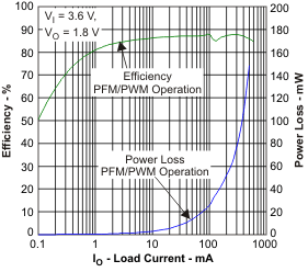
Efficiency vs. Load Current
