SLVSCQ0B June   2015  – March 2021 TPS62743

PRODUCTION DATA  

  1. Features
  2. Applications
  3. Description
  4. Revision History
  5. Device Comparison Table
  6. Pin Configuration and Functions
  7. Specifications
    1. 7.1 Absolute Maximum Ratings
    2. 7.2 ESD Ratings
    3. 7.3 Recommended Operating Conditions
    4. 7.4 Thermal Information
    5. 7.5 Electrical Characteristics
    6. 7.6 Timing Requirements
    7. 7.7 Typical Characteristics
  8. Detailed Description
    1. 8.1 Overview
    2. 8.2 Functional Block Diagram
    3. 8.3 Feature Description
      1. 8.3.1 DCS-Control™
      2. 8.3.2 Power Save Mode Operation
      3. 8.3.3 Output Voltage Selection
      4. 8.3.4 Output Voltage Discharge of the Buck Converter
      5. 8.3.5 Undervoltage Lockout UVLO
      6. 8.3.6 Short circuit protection
    4. 8.4 Device Functional Modes
      1. 8.4.1 Enable and Shutdown
      2. 8.4.2 Device Start-up and Softstart
      3. 8.4.3 Automatic Transition Into No Ripple 100% Mode
  9. Application and Implementation
    1. 9.1 Application Information
    2. 9.2 Typical Application
      1. 9.2.1 Design Requirements
      2. 9.2.2 Detailed Design Procedure
        1. 9.2.2.1 Inductor Selection
        2. 9.2.2.2 Output Capacitor Selection
        3. 9.2.2.3 Input Capacitor Selection
      3. 9.2.3 Application Curves
    3. 9.3 System Example
  10. 10Power Supply Recommendations
  11. 11Layout
    1. 11.1 Layout Guidelines
    2. 11.2 Layout Example
  12. 12Device and Documentation Support
    1. 12.1 Device Support
      1. 12.1.1 Third-Party Products Disclaimer
    2. 12.2 Receiving Notification of Documentation Updates
    3. 12.3 Support Resources
    4. 12.4 Trademarks
    5. 12.5 Electrostatic Discharge Caution
    6. 12.6 Glossary
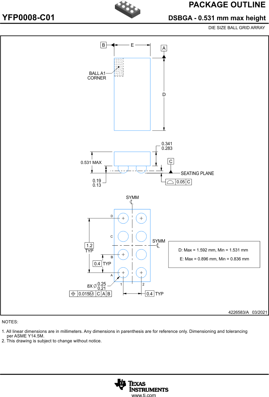
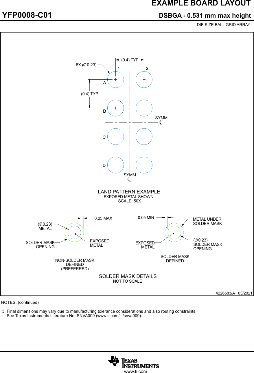
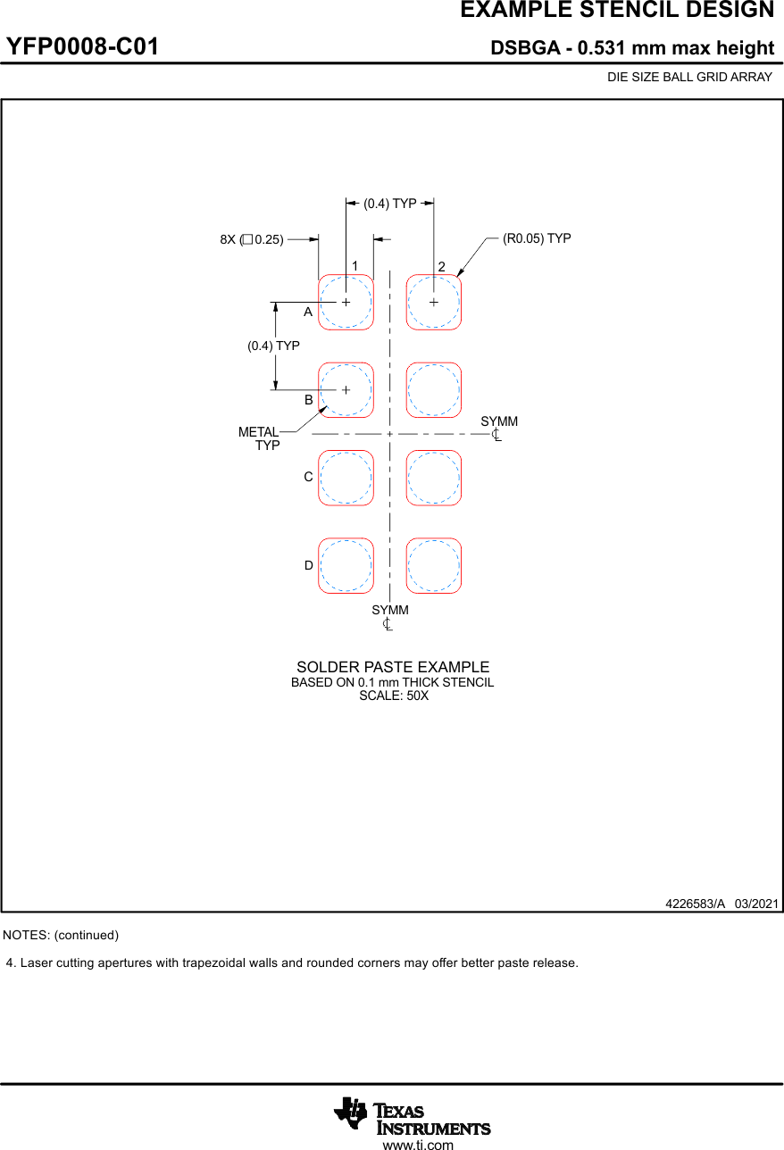
  13. 13Mechanical, Packaging, and Orderable Information

Package Options

Refer to the PDF data sheet for device specific package drawings

Mechanical Data (Package|Pins)
  • YFP|8
Thermal pad, mechanical data (Package|Pins)
Orderable Information

Mechanical, Packaging, and Orderable Information

The following pages include mechanical, packaging, and orderable information. This information is the most current data available for the designated devices. This data is subject to change without notice and revision of this document. For browser-based versions of this data sheet, refer to the left-hand navigation.

GUID-20210310-CA0I-QFNV-7HH9-6HMD3FGP8SLX-low.gif
GUID-20210310-CA0I-6P7T-CD45-LBGZXCP4X4TJ-low.gif
GUID-20210310-CA0I-ZTKM-0BTF-MPMPVCT8L1RM-low.gif