SLVSCQ0B June 2015 – March 2021 TPS62743
PRODUCTION DATA
- 1 Features
- 2 Applications
- 3 Description
- 4 Revision History
- 5 Device Comparison Table
- 6 Pin Configuration and Functions
- 7 Specifications
- 8 Detailed Description
- 9 Application and Implementation
- 10Power Supply Recommendations
- 11Layout
- 12Device and Documentation Support
- 13Mechanical, Packaging, and Orderable Information
Package Options
Refer to the PDF data sheet for device specific package drawings
Mechanical Data (Package|Pins)
- YFP|8
Thermal pad, mechanical data (Package|Pins)
Orderable Information
9.2.2.1 Inductor Selection
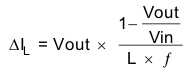
The inductor value affects the peak-to-peak ripple current, the PWM-to-PFM transition point, the output voltage ripple and the efficiency. The selected inductor has to be rated for its DC resistance and saturation current. The inductor ripple current (ΔIL) decreases with higher inductance and increases with higher VIN or VOUT and can be estimated according to Equation 1.
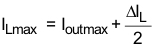
Equation 2 calculates the maximum inductor current under static load conditions. The saturation current of the inductor should be rated higher than the maximum inductor current, as calculated with equation 2. This is recommended because during a heavy load transient the inductor current rises above the calculated value. A more conservative way is to select the inductor saturation current according to the high-side MOSFET switch current limit, ILIMF.
where
- f = Switching Frequency
- L = Inductor Value
- ΔIL= Peak to Peak inductor ripple current
- ILmax = Maximum Inductor current
Table 9-3 shows a list of possible inductors.
| INDUCTANCE [µH] | DIMENSIONS [mm3] | INDUCTOR TYPE | Isat/DCR | SUPPLIER(1) | Comment | |
|---|---|---|---|---|---|---|
| 2.2 | 2.0 x 1.6 x 1.0 | DFE201610C | 1.4 A/170 mΩ | TOKO | Efficiency plot Figure 9-9 | |
| 2.2 | 2.0 × 1.25 × 1.0 | MIPSZ2012D 2R2 | 0.7 A/230 mΩ | FDK | ||
| 2.2 | 2.0 x 1.2 x 1.0 | 744 797 752 22 | 0.7 A/200 mΩ | Würth Elektronik | ||
| 2.2 | 1.6 x 0.8 x 0.8 | MDT1608-CH2R2M | 0.7 A/300 mΩ | TOKO | ||