SLVSDD1F December   2017  – June 2022 TPS62800 , TPS62801 , TPS62802 , TPS62806 , TPS62807 , TPS62808

PRODUCTION DATA  

  1. Features
  2. Applications
  3. Description
  4. Revision History
  5. Device Comparison Table
  6. Pin Configuration and Functions
  7. Specifications
    1. 7.1 Absolute Maximum Ratings
    2. 7.2 ESD Ratings
    3. 7.3 Recommended Operating Conditions
    4. 7.4 Thermal Information
    5. 7.5 Electrical Characteristics
    6. 7.6 Typical Characteristics
  8. Detailed Description
    1. 8.1 Overview
    2. 8.2 Functional Block Diagram
    3. 8.3 Feature Description
      1. 8.3.1 Smart Enable and Shutdown (EN)
      2. 8.3.2 Soft Start
      3. 8.3.3 VSEL/MODE Pin
        1. 8.3.3.1 Output Voltage Selection (R2D Converter)
        2. 8.3.3.2 Mode Selection — Power Save Mode and Forced PWM Operation
      4. 8.3.4 Undervoltage Lockout (UVLO)
      5. 8.3.5 Switch Current Limit and Short Circuit Protection
      6. 8.3.6 Thermal Shutdown
      7. 8.3.7 Output Voltage Discharge
    4. 8.4 Device Functional Modes
      1. 8.4.1 Power Save Mode Operation
      2. 8.4.2 Forced PWM Mode Operation
      3. 8.4.3 100% Mode Operation
      4. 8.4.4 Optimized Transient Performance from PWM-to-PFM Mode Operation
  9. Application and Implementation
    1. 9.1 Application Information
    2. 9.2 Typical Application
      1. 9.2.1 Design Requirements
      2. 9.2.2 Detailed Design Procedure
        1. 9.2.2.1 Custom Design With WEBENCH® Tools
        2. 9.2.2.2 Inductor Selection
        3. 9.2.2.3 Output Capacitor Selection
        4. 9.2.2.4 Input Capacitor Selection
      3. 9.2.3 Application Curves
    3. 9.3 System Examples
  10. 10Power Supply Recommendations
  11. 11Layout
    1. 11.1 Layout Guidelines
    2. 11.2 Layout Example
  12. 12Device and Documentation Support
    1. 12.1 Device Support
      1. 12.1.1 Third-Party Products Disclaimer
      2. 12.1.2 Development Support
        1. 12.1.2.1 Custom Design With WEBENCH® Tools
    2. 12.2 Receiving Notification of Documentation Updates
    3. 12.3 Support Resources
    4. 12.4 Trademarks
    5. 12.5 Electrostatic Discharge Caution
    6. 12.6 Glossary
  13. 13Mechanical, Packaging, and Orderable Information

Package Options

Mechanical Data (Package|Pins)
Thermal pad, mechanical data (Package|Pins)
Orderable Information

Application Curves

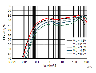
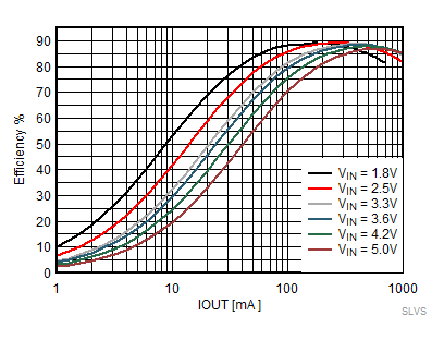
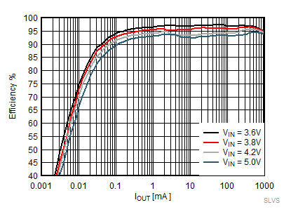
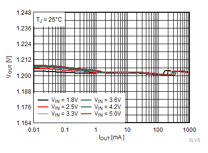
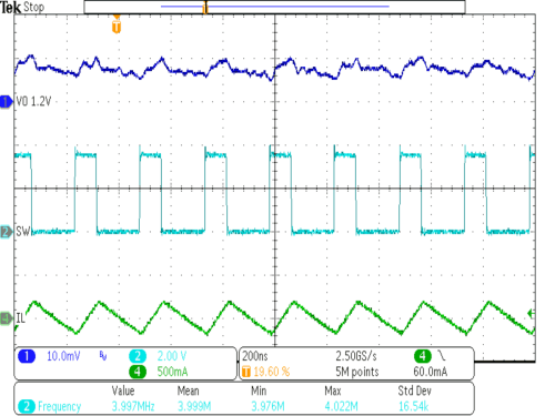
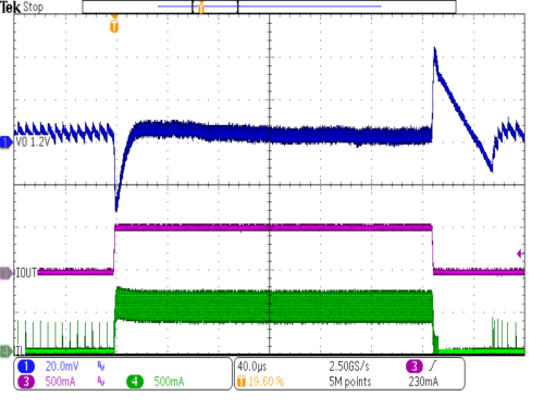
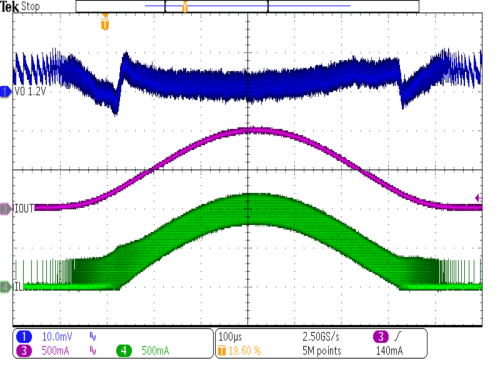
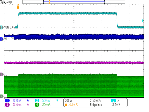
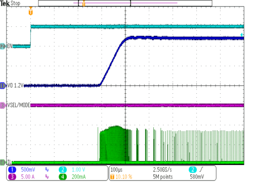
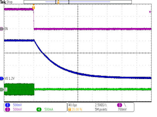
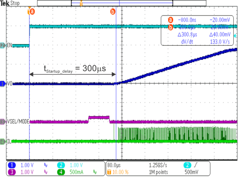
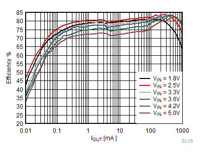
The conditions for the below application curves are VIN = 3.6 V, VOUT = 1.2 V, and the components listed in Table 9-1, unless otherwise noted.
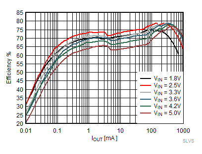
GUID-F936527B-E67C-48A6-9CE8-6851B73B597C-low.gif
TPS62800RVSEL = 10 kΩ to GND
Figure 9-2 Efficiency Power Save Mode
VOUT = 0.4 V
GUID-0746CACF-5C0B-4FFE-A78C-09719245232D-low.gif
TPS62801RVSEL = 10 kΩ to GND
Figure 9-4 Efficiency Power Save Mode
VOUT = 0.8 V
GUID-23A3EBCF-97C1-4E68-A9E1-DC958FD26D11-low.gif
TPS62801RVSEL = 56.2 kΩ
VSEL/MODE pin = high after start-up
Figure 9-6 Efficiency Forced PWM Mode
VOUT = 1.2 V
GUID-DAE22761-3782-4112-8FEE-E5F6115FB19B-low.gif
TPS62801VSEL/MODE = GND, VOUT = 1.2 V
Figure 9-8 Inductor Comparison
GUID-9EFAC2D2-DF51-416B-B0B4-60B47CFE5E8A-low.gif
TPS628023.3 V VOUT, VSEL/MODE = 249 k
Figure 9-10 Efficiency Power Save Mode
VOUT = 3.3 V
GUID-5B8C6BF7-0970-4984-99FD-9D5D96088897-low.gif
TPS62807VOUT = 1.2 V, VSEL/MODE = GND
L = 1-µH DFE201610E
Figure 9-12 Efficiency Power Save Mode
VOUT = 1.2 V
GUID-F504ADB6-E88B-4C65-A3B7-5082CBA708BB-low.gif
TPS62801VSEL/MODE = GND
VOUT = 1.2 VPFM/PWM modeTJ = 25°C
Figure 9-14 Output Voltage vs Output Current
GUID-6882844A-D766-461D-9B18-3AD50B7BBFF8-low.gif
TPS62801VSEL/MODE = GND
VOUT = 1.2 VPFM/PWM modeTJ = 85°C
Figure 9-16 Output Voltage vs Output Current
GUID-48A474CA-4887-4F29-9B96-90D90C68BB9E-low.gif
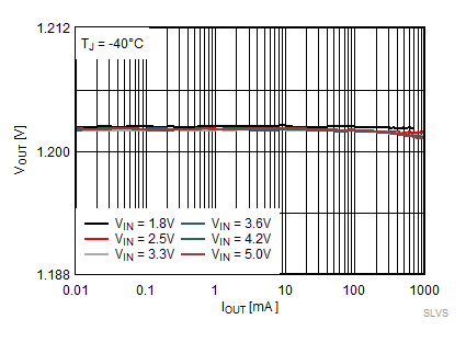
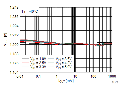
TPS62801VSEL/MODE = high after start-up
VOUT = 1.2 VForced PWM modeTJ = –40°C
Figure 9-18 Output Voltage vs Output Current
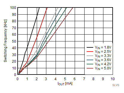
GUID-B683D5F1-03CC-4114-85C2-C0A56BCA0394-low.gif
TPS62801VSEL/MODE = GND
VOUT = 1.2 VPFM/PWM modeTJ = 25°C
Figure 9-20 Switching Frequency vs Output Current
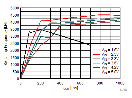
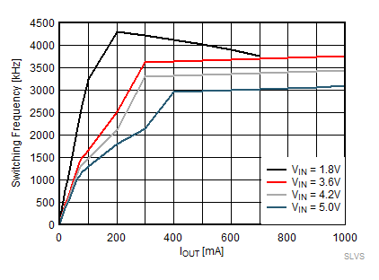
GUID-783929FD-E3EA-4E66-B5B2-C67138A1B9C8-low.gif
TPS62801VSEL/MODE = high after start-up
VOUT = 1.2 VForced PWM ModeTJ = 25°C
Figure 9-22 Switching Frequency vs Output Current
GUID-336BBD42-5BA2-4B53-A7E4-0B92A39D609D-low.gif
TPS62806 VSEL/MODE = GND L = 1 µH
VOUT = 0.7 V PFM/PWM mode TJ = 25°C
Figure 9-24 Switching Frequency vs Output Current
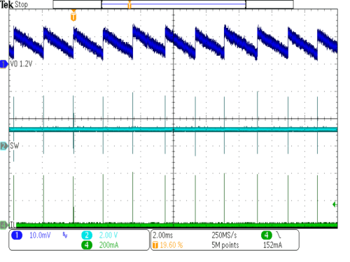
GUID-9E679E7C-75F0-4009-9A0F-2A6C514C59C7-low.gif
TPS62801 VOUT = 1.2 V VSEL/MODE = GND
IOUT = 10 mA PFM mode
Figure 9-26 Typical Operation Power Save Mode
GUID-E2E4632C-F184-4D13-9FD1-6E675FABA361-low.gif
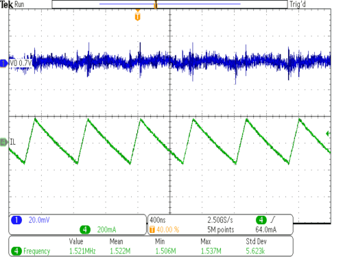
VOUT = 0.7 V IOUT = 0 mA VSEL/MODE = VIN (after start-up)
VIN = 3.8 V PFM Mode, L = 1-µH DFE201610E
Figure 9-28 TPS62806 Typical Forced PWM Mode Operation (1.5 MHz)
GUID-CE65ED24-B1DB-42E5-83DA-90B6AA79AE0D-low.gif
Forced PWM mode VOUT = 1.2 V IOUT = 0 mA
VSEL/MODE = VIN (after start-up)
Figure 9-30 TPS62801 Typical Operation Forced PWM Mode
GUID-404F7331-3A86-4B1B-B299-CF9A7373B2C7-low.gif
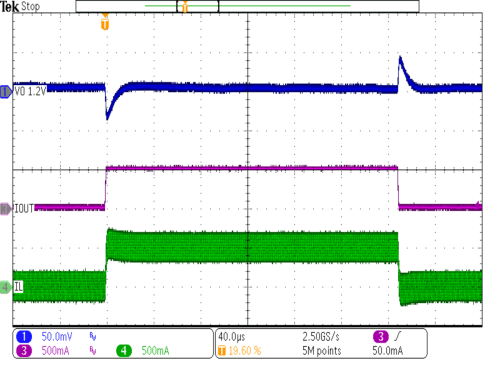
TPS62801 VOUT = 1.2 V VSEL/MODE = GND
rise / fall time < 1 µs PFM / PWM mode
IOUT = 5 mA to 500 mA
Figure 9-32 Load Transient Power Save Mode
GUID-A7995474-4AB9-4715-ADAE-FCEA000DC19D-low.gif
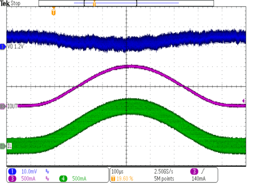
TPS62801VOUT = 1.2 VVSEL/MODE = GND
IOUT = 1 mA to 1 A 1 kHzPFM/PWM mode
Figure 9-34 AC Load Sweep Power Save Mode
GUID-7741CB06-6AC3-430B-8962-3CDDE0F9C127-low.gif
TPS62801VOUT = 1.2 VVIN = 3.6 V to 4.2 V
rise / fall time = 10 µsIOUT = 50 mA
Figure 9-36 Line Transient PFM Mode
GUID-2FD21EB4-5BEE-4220-8C1A-1E84841016D0-low.gif
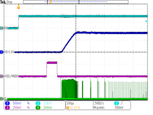
VOUT = 0.8 V VSEL/MODE = Low (through RVSEL)
RVSEL = 10 kΩ RLoad = 220 Ω
Figure 9-38 TPS62801 Start-Up, VOUT = 0.8 V
GUID-68ACCF44-94A5-4D66-82D1-9FE35C7EC2D9-low.gif
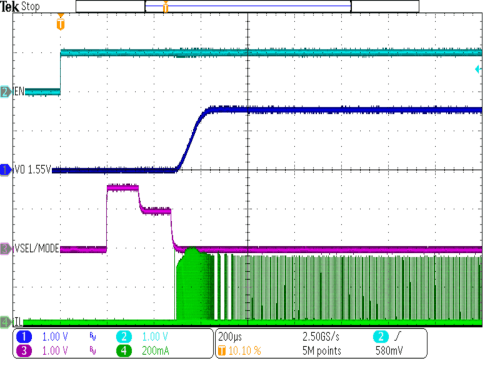
VOUT = 1.55 V VSEL/MODE = Low (through RVSEL)
RLoad = 220 Ω RVSEL = 249 kΩ
Figure 9-40 TPS62801 Start-Up, VOUT = 1.55 V
GUID-055E55A6-424A-40C4-B528-9F0D8C569D1F-low.gif
VSEL/MODE = GND
Figure 9-42 Start-Up Delay Time, VSEL = 0
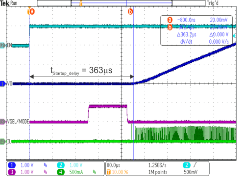
GUID-C930FFCE-08C6-42D3-B49E-77C643E736D4-low.gif
RVSEL = 36.5 kΩ
Figure 9-44 Start-Up Delay Time, VSEL = 7
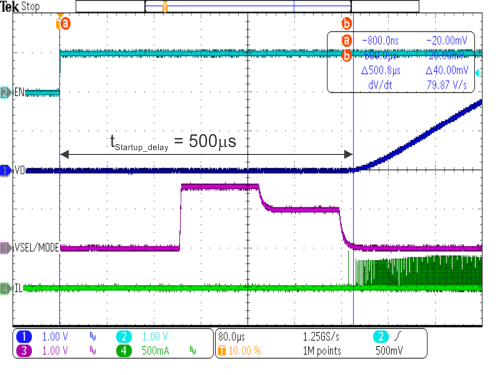
GUID-F5B9BBEF-D4C7-4DB1-ADEF-94C1E82AA330-low.gif
RVSEL = 249 kΩ
Figure 9-46 Start-Up Delay Time, VSEL = 16
GUID-E6FCEA63-AAD2-4493-84D7-151522B5B015-low.gif
TPS62800VSEL/MODE = GND
Figure 9-3 Efficiency Power Save Mode
VOUT = 0.7 V
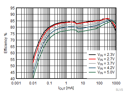
GUID-E51D1205-3CF3-438E-BC82-6BFBEF1ED73C-low.gif
TPS62801RVSEL = 15.4 kΩ to GND
Figure 9-5 Efficiency Power Save Mode
VOUT = 0.9 V
GUID-996CABBE-CA09-477F-97CC-4DFE371B693B-low.gif
TPS62801VSEL/MODE = GND
Figure 9-7 Efficiency Power Save Mode
VOUT = 1.2 V
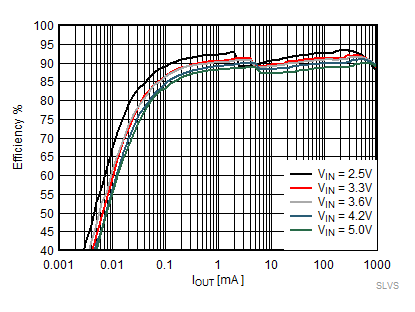
GUID-3C3715E1-1C40-4FD8-A495-DB50202B9297-low.gif
TPS62802 VSEL/MODE = GND
Figure 9-9 Efficiency Power Save Mode
VOUT = 1.8 V
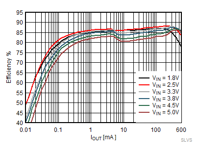
GUID-C072C1E0-F941-4203-BDE1-77CB565225C8-low.gif
TPS62806 VOUT = 0.7 V, VSEL/MODE = GND
L = 1-µH DFE201610E
Figure 9-11 Efficiency Power Save Mode
VOUT = 0.7 V
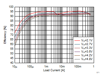
GUID-838DD3D8-8939-457A-B69E-43D3FC62173F-low.gif
TPS62808VOUT = 1.8 V, VSEL/MODE = GND
L = 1-µH DFE201610E
Figure 9-13 Efficiency Power Save Mode
VOUT = 1.8 V
GUID-5FB33FA7-CFA1-4333-A28C-6057C6F9C599-low.gif
TPS62801VSEL/MODE = GND
VOUT = 1.2 VPFM/PWM modeTJ = –40°C
Figure 9-15 Output Voltage vs Output Current
GUID-9E5AEEEA-7B49-457C-9AD5-FF58B7625A93-low.gif
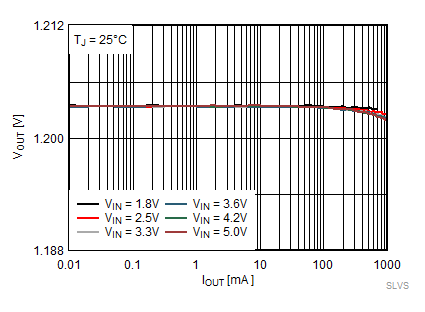
TPS62801VSEL/MODE = high after start-up
VOUT = 1.2 VForced PWM modeTJ = 25°C
Figure 9-17 Output Voltage vs Output Current
GUID-F81E28D8-DFEF-43FD-81CE-13BF995E67D5-low.gif
TPS62801VSEL/MODE = high after start-up
VOUT = 1.2 VForced PWM modeTJ = 85°C
Figure 9-19 Output Voltage vs Output Current
GUID-BEB5643D-C151-4C5E-85D3-9C3A78F98DF1-low.gif
TPS62801VSEL/MODE = GND
VOUT = 1.2 VPFM/PWM modeTJ = 25°C
Figure 9-21 Switching Frequency (Zoom In)
GUID-27C89B8A-3581-4A85-B0AD-40DE635173E5-low.gif
TPS62801VSEL/MODE = 10 kΩ to GND
VOUT = 0.8 VPFM/PWM modeTJ = 25°C
Figure 9-23 Switching Frequency vs Output Current
GUID-04E2BF3A-11FA-45F1-A1F4-F5DD3AB62CF6-low.gif
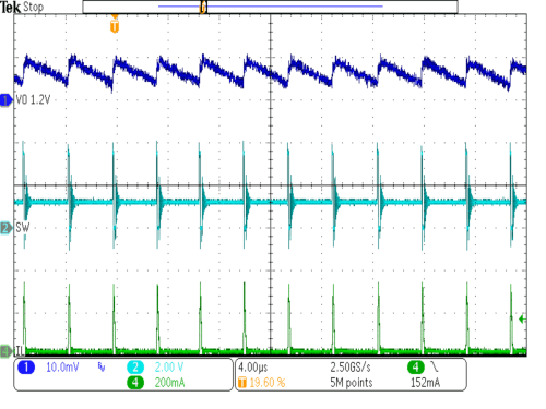
TPS62801 VOUT = 1.2 V VSEL/MODE = GND
IOUT = 25 µA PFM mode
Figure 9-25 Typical Operation Power Save Mode
GUID-62F95FD5-B4B7-4BB6-BC91-B77AE6F8EAA6-low.gif
VOUT = 0.7 VIOUT = 10 mAVSEL/MODE = GND
VIN = 3.8 VPFM Mode, L = 1-µH DFE201610E
Figure 9-27 TPS62806 Typical Operation Power Save Mode
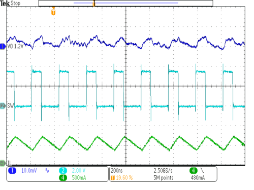
GUID-51972E74-8085-4FAB-AD75-96DB09F3FF9A-low.gif
PWM modeVOUT = 1.2 VVSEL/MODE = GND
IOUT = 500 mA
Figure 9-29 TPS62801 Typical Operation PWM Mode
GUID-16D32EB9-1113-4F1B-9E70-D4DC9AEF1FF2-low.gif
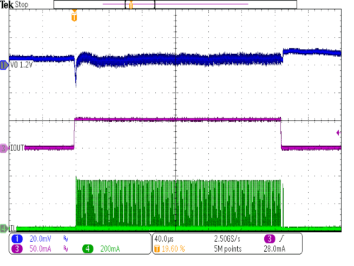
TPS62801 VOUT = 1.2 V VSEL/MODE = GND
rise / fall time < 1 µs IOUT = 0 mA to 50 mA, PFM Mode
Figure 9-31 Load Transient Power Save Mode
GUID-C0BE50B3-1D2B-4027-8769-4599E718763A-low.gif
Forced PWM mode VOUT = 1.2 V VSEL/MODE = VIN (after start-up)
rise / fall time < 1 µs IOUT = 5 mA to 500 mA
Figure 9-33 TPS62801 Load Transient Forced PWM Mode
GUID-4641F198-0D06-4ECE-AD02-1AA1A810024B-low.gif
TPS62801VOUT = 1.2 VVSEL/MODE = VIN
IOUT = 1 mA to 1 A, 1 kHz(after start-up)
Forced PWM mode
Figure 9-35 AC Load Sweep Forced PWM Mode
GUID-EBE20777-A715-4F83-9826-DB09D9553EF3-low.gif
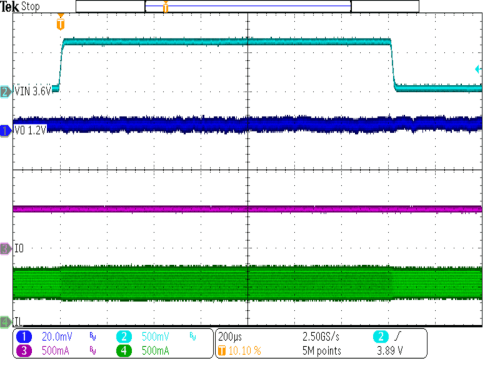
TPS62801VOUT = 1.2 VVIN = 3.6 V to 4.2 V
rise / fall time = 10 µsIOUT = 500 mA
Figure 9-37 Line Transient PWM Mode
GUID-2A45AE7D-DD9F-4F67-8A11-9E043C0609B6-low.gif
TPS62801VOUT = 1.2 VVSEL/MODE = GND
RLoad = 220 Ω
Figure 9-39 Start-Up, VOUT = 1.2 V
GUID-2B037859-9233-49D6-9A27-05AA0B89B517-low.gif
TPS62801VOUT = 1.2 VVSEL/MODE = VIN
EN = high to lowNo load
Figure 9-41 Output Discharge
GUID-1EDD3A80-D5B0-459C-ADDB-0B9E1B4BF2AE-low.gif
RVSEL = 10 kΩ
Figure 9-43 Start-Up Delay Time, VSEL = 1
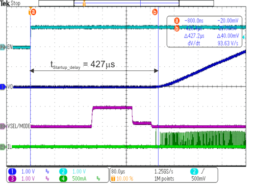
GUID-16DBB2FA-812F-4BD2-89BD-E81931152E3C-low.gif
RVSEL = 44.2 kΩ
Figure 9-45 Start-Up Delay Time, VSEL = 8