SLVSDU1K August 2018 – July 2025 TPS62810-Q1 , TPS62811-Q1 , TPS62812-Q1 , TPS62813-Q1
PRODUCTION DATA
- 1
- 1 Features
- 2 Applications
- 3 Description
- 4 Device Comparison Table
- 5 Pin Configuration and Functions
- 6 Specifications
- 7 Parameter Measurement Information
- 8 Detailed Description
- 9 Application and Implementation
- 10Device and Documentation Support
- 11Revision History
- 12Mechanical, Packaging, and Orderable Information
Package Options
Mechanical Data (Package|Pins)
- RWY|9
Thermal pad, mechanical data (Package|Pins)
- RWY|9
Orderable Information
9.3.2 Voltage Tracking
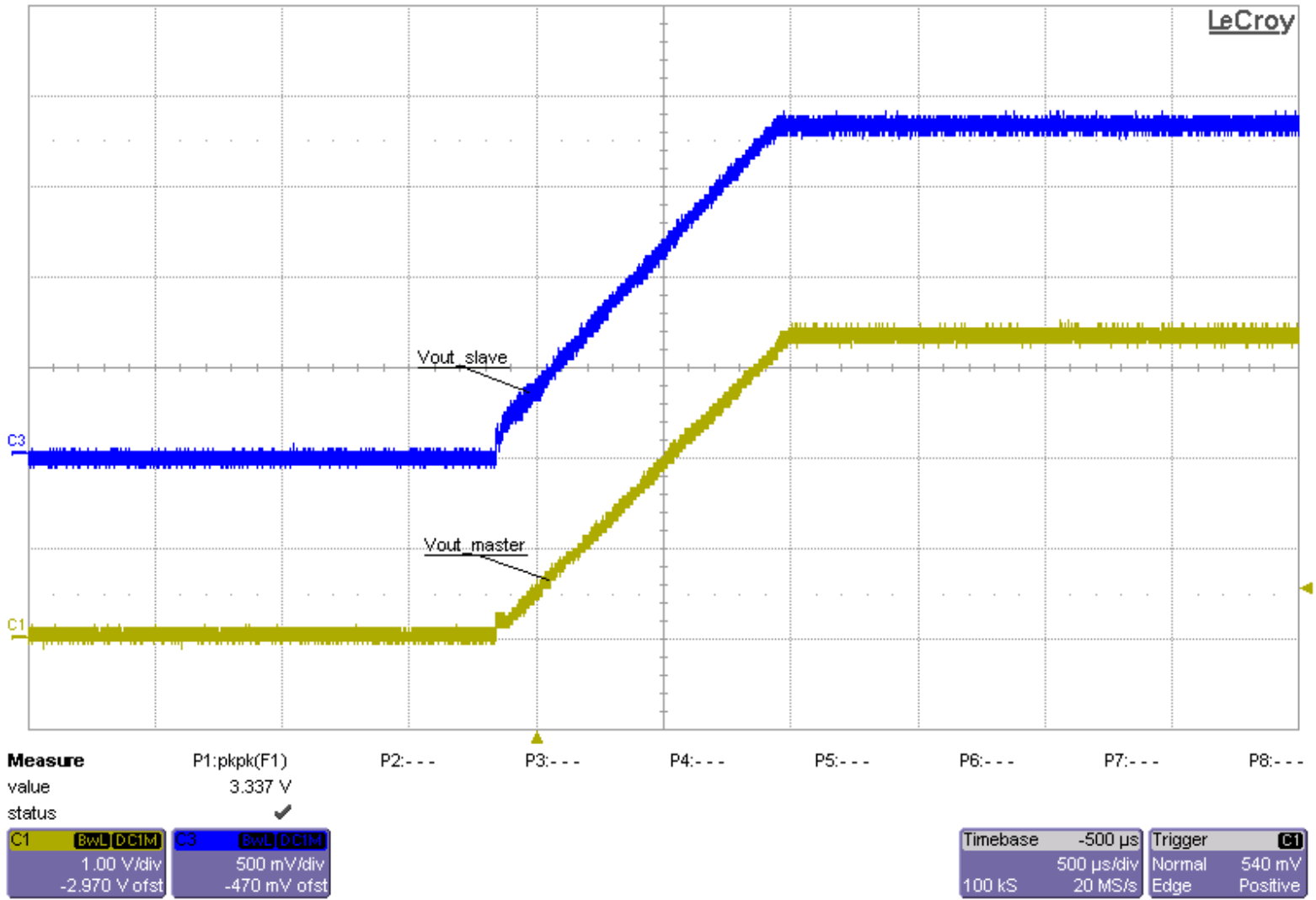
The TPS6281x-Q1 follows the voltage applied to the SS/TR pin. A voltage ramp on SS/TR to 0.6 V ramps the output voltage according to the 0.6 V feedback voltage.
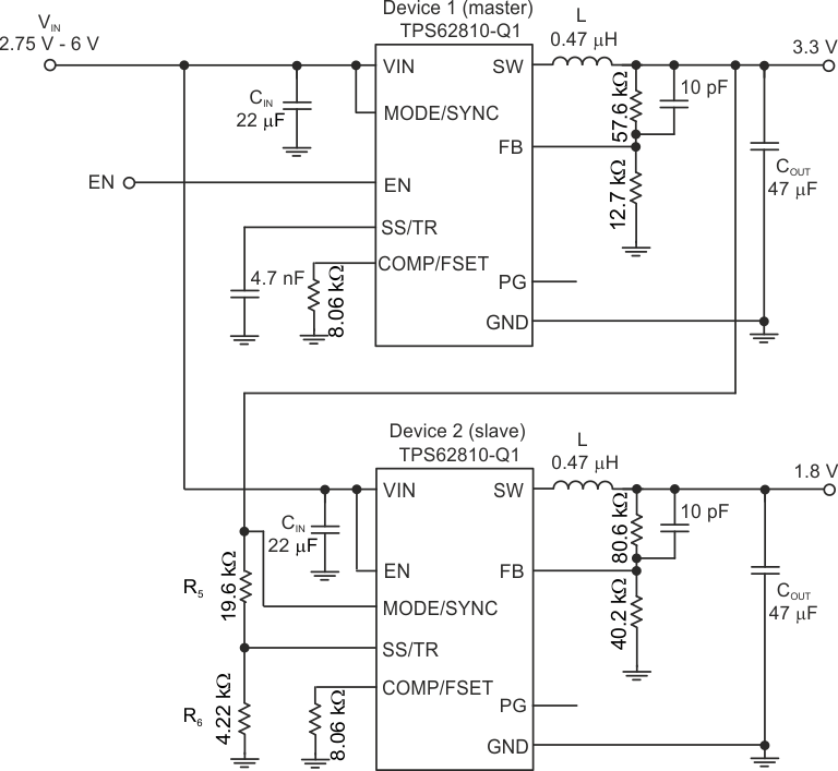
Tracking the 3.3 V of device 1, such that both rails reach the target voltage at the same time, requires a resistor divider on SS/TR of device 2 equal to the output voltage divider of device 1. The output current of 2.5 µA on the SS/TR pin causes an offset voltage on the resistor divider formed by R5 and R6. The equivalent resistance of R5 // R6, so keep below 15 kΩ. The current from SS/TR causes a slightly higher voltage across R6 than 0.6 V, which is desired because device 2 switches to the internal reference as soon as the voltage at SS/TR is higher than 0.6 V.
In case both devices must run in forced PWM mode, TI recommends to tie the MODE pin of device 2 to the output voltage or the power good signal of device 1, the controller device. The TPS6281x-Q1 has a duty cycle limitation defined by the minimum on-time. For tracking down to low output voltages, device 2 cannot follow after the minimum duty cycle is reached. Enabling PFM mode while tracking is in progress allows the user to ramp down the output voltage close to 0 V.
 Figure 9-58 Schematic for Output Voltage Tracking
 Figure 9-59 Scope Plot for Output Voltage Tracking