SLVSDU1K August   2018  – July 2025 TPS62810-Q1 , TPS62811-Q1 , TPS62812-Q1 , TPS62813-Q1

PRODUCTION DATA  

  1.   1
  2. Features
  3. Applications
  4. Description
  5. Device Comparison Table
  6. Pin Configuration and Functions
  7. Specifications
    1. 6.1 Absolute Maximum Ratings
    2. 6.2 ESD Ratings
    3. 6.3 Recommended Operating Conditions
    4. 6.4 Thermal Information
    5. 6.5 Electrical Characteristics
    6. 6.6 Typical Characteristics
  8. Parameter Measurement Information
    1. 7.1 Schematic
  9. Detailed Description
    1. 8.1 Overview
    2. 8.2 Functional Block Diagram
    3. 8.3 Feature Description
      1. 8.3.1 Precise Enable
      2. 8.3.2 COMP/FSET
      3. 8.3.3 MODE / SYNC
      4. 8.3.4 Spread Spectrum Clocking (SSC)
      5. 8.3.5 Undervoltage Lockout (UVLO)
      6. 8.3.6 Power Good Output (PG)
      7. 8.3.7 Thermal Shutdown
    4. 8.4 Device Functional Modes
      1. 8.4.1 Pulse Width Modulation (PWM) Operation
      2. 8.4.2 Power Save Mode Operation (PWM/PFM)
      3. 8.4.3 100% Duty-Cycle Operation
      4. 8.4.4 Current Limit and Short-Circuit Protection
      5. 8.4.5 Foldback Current Limit and Short-Circuit Protection
      6. 8.4.6 Output Discharge
      7. 8.4.7 Soft Start / Tracking (SS/TR)
  10. Application and Implementation
    1. 9.1 Application Information
      1. 9.1.1 Programming the Output Voltage
      2. 9.1.2 External Component Selection
        1. 9.1.2.1 Inductor Selection
      3. 9.1.3 Capacitor Selection
        1. 9.1.3.1 Input Capacitor
        2. 9.1.3.2 Output Capacitor
    2. 9.2 Typical Application
      1. 9.2.1 Design Requirements
      2. 9.2.2 Detailed Design Procedure
      3. 9.2.3 Application Curves
    3. 9.3 System Examples
      1. 9.3.1 Fixed Output Voltage Versions
      2. 9.3.2 Voltage Tracking
      3. 9.3.3 Synchronizing to an External Clock
    4. 9.4 Power Supply Recommendations
    5. 9.5 Layout
      1. 9.5.1 Layout Guidelines
      2. 9.5.2 Layout Example
  11. 10Device and Documentation Support
    1. 10.1 Device Support
      1. 10.1.1 Third-Party Products Disclaimer
    2. 10.2 Documentation Support
      1. 10.2.1 Related Documentation
    3. 10.3 Receiving Notification of Documentation Updates
    4. 10.4 Support Resources
    5. 10.5 Trademarks
    6. 10.6 Electrostatic Discharge Caution
    7. 10.7 Glossary
  12. 11Revision History
  13. 12Mechanical, Packaging, and Orderable Information

Package Options

Mechanical Data (Package|Pins)
Thermal pad, mechanical data (Package|Pins)
Orderable Information

Fixed Output Voltage Versions

Versions with an internally fixed output voltage allow the user remove the external feedback voltage divider. This ability not only allows the user reduce the total design size but also provides higher accuracy as there is no additional error caused by the external resistor divider. The FB pin must be tied to the output voltage directly as shown in Figure 9-57. Independent of that, the application shown runs with an internally defined switching frequency of 2.25 MHz by connecting COMP/FSET to GND.
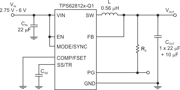
TPS62810-Q1 TPS62811-Q1 TPS62812-Q1 TPS62813-Q1 Schematic for Fixed Output Voltage VersionsFigure 9-57 Schematic for Fixed Output Voltage Versions