SLVSFM8 March 2021 TPS62810M , TPS62811M , TPS62812M , TPS62813M
PRODUCTION DATA
- 1 Features
- 2 Applications
- 3 Description
- 4 Revision History
- 5 Device Comparison Table
- 6 Pin Configuration and Functions
- 7 Specifications
- 8 Parameter Measurement Information
- 9 Detailed Description
- 10Application and Implementation
- 11Power Supply Recommendations
- 12Layout
- 13Device and Documentation Support
- 14Mechanical, Packaging, and Orderable Information
Package Options
Mechanical Data (Package|Pins)
- RWY|9
Thermal pad, mechanical data (Package|Pins)
- RWY|9
Orderable Information
8.1 Schematic
 Figure 8-1 Measurement Setup for
TPS62810M (4 A) and TPS62813M (3 A)
Figure 8-1 Measurement Setup for
TPS62810M (4 A) and TPS62813M (3 A)Table 8-1 List of Components
| REFERENCE | DESCRIPTION | MANUFACTURER (1) |
|---|---|---|
| IC | TPS62810M or TPS62813M | Texas Instruments |
| L | 0.47-µH inductor; XEL4030-471MEB | Coilcraft |
| CIN | 22 µF / 10 V; GCM31CR71A226KE02L | Murata |
| COUT | 2 × 22 µF / 10 V; GCM31CR71A226KE02L + 1 × 10 µF, 6.3 V; GCM188D70J106ME36 | Murata |
| CSS | 4.7 nF (equal to 1-ms start-up ramp) | Any |
| RCF | 8.06 kΩ | Any |
| CFF | 10 pF | Any |
| R1 | Depending on VOUT | Any |
| R2 | Depending on VOUT | Any |
| R3 | 100 kΩ | Any |
(1) See the Third-party Products Disclaimer.
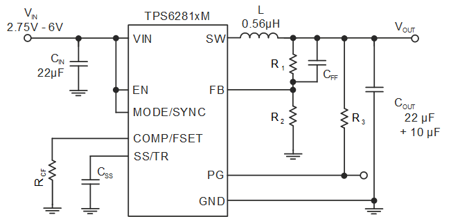
 Figure 8-2 Measurement Setup for TPS62811M (1 A) and TPS62812M (2 A)
Table 8-2 List of Components
| REFERENCE | DESCRIPTION | MANUFACTURER (1) |
|---|---|---|
| IC | TPS62812M or TPS62811M | Texas Instruments |
| L | 0.56-µH inductor; XEL4020-561MEB | Coilcraft |
| CIN | 22 µF / 10 V; GCM31CR71A226KE02L | Murata |
| COUT | 1 × 22 µF / 10 V; GCM31CR71A226KE02L + 1 × 10 µF, 6.3 V; GCM188D70J106ME36 |
Murata |
| CSS | 4.7 nF (equal to 1-ms start-up ramp) | Any |
| RCF | 8.06 kΩ | Any |
| CFF | 10 pF | Any |
| R1 | Depending on VOUT | Any |
| R2 | Depending on VOUT | Any |
| R3 | 100 kΩ | Any |
(1) See the Third-party Products Disclaimer.
Table 8-3 List of Key Components, Operation at
–55°C
| REFERENCE | DESCRIPTION | MANUFACTURER(1) |
|---|---|---|
| IC | TPS62810M, TPS62811M, TPS62812M, or TPS62813M | Texas Instruments |
| L | 0.47-µH inductor; TFM252012ALMAR47MTAA | TDK |
| CIN | 22 µF / 10 V; GCJ31CL8ED226KE07 | Murata |
| COUT | 2 × 22 µF / 10 V; GCJ31CL8ED226KE07 + 1 × 10 µF, 16 V; GCJ32ER91C106KE01 | Murata |
(1) See the Third-party Products Disclaimer.