SLVSDU1J August 2018 – March 2023 TPS62810-Q1 , TPS62811-Q1 , TPS62812-Q1 , TPS62813-Q1
PRODUCTION DATA
- 1 Features
- 2 Applications
- 3 Description
- 4 Revision History
- 5 Device Comparison Table
- 6 Pin Configuration and Functions
- 7 Specifications
- 8 Parameter Measurement Information
- 9 Detailed Description
- 10Application and Implementation
- 11Device and Documentation Support
- 12Mechanical, Packaging, and Orderable Information
Package Options
Mechanical Data (Package|Pins)
- RWY|9
Thermal pad, mechanical data (Package|Pins)
- RWY|9
Orderable Information
3 Description
The TPS6281x-Q1 is family of pin-to-pin 1-A, 2-A, 3-A, and 4-A synchronous step-down DC/DC converters. All devices offer high efficiency and ease of use. The TPS6281x-Q1 family is based on a peak current mode control topology. The TPS6281x-Q1 is designed for automotive applications such as infotainment and advanced driver assistance systems. Low resistive switches allow up to 4-A continuous output current at high ambient temperature. The switching frequency is externally adjustable from 1.8 MHz to 4 MHz and can also be synchronized to an external clock in the same frequency range. In PWM/PFM mode, the TPS6281x-Q1 automatically enter power save mode at light loads to maintain high efficiency across the whole load range. The TPS6281x-Q1 provide 1% output voltage accuracy in PWM mode which helps design a power supply with high output voltage accuracy. The SS/TR pin allows setting the start-up time or forming tracking of the output voltage to an external source. This feature allows external sequencing of different supply rails and limiting the inrush current during start-up.
The TPS6281x-Q1 is available in a 3-mm × 2-mm VQFN package with wettable flanks.
| PART NUMBER | PACKAGE(1) | BODY SIZE (NOM) |
|---|---|---|
| TPS62810-Q1 | RWY (VQFN, 9) | 3.00 mm × 2.00 mm |
| TPS62811-Q1 | ||
| TPS62812-Q1 | ||
| TPS62813-Q1 |
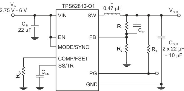
 Simplified Schematic
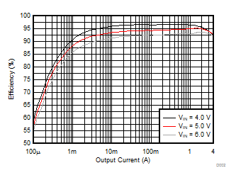
 Efficiency vs Output Current; VOUT = 3.3 V; PWM/PFM; fS = 2.25 MHz