SLUSDM1A March 2020 – December 2021 TPS62816-Q1
PRODUCTION DATA
- 1 Features
- 2 Applications
- 3 Description
- 4 Revision History
- 5 Device Comparison Table
- 6 Pin Configuration and Functions
- 7 Specifications
- 8 Parameter Measurement Information
- 9 Detailed Description
- 10Application and Implementation
- 11Power Supply Recommendations
- 12Layout
- 13Device and Documentation Support
- 14Mechanical, Packaging, and Orderable Information
Package Options
Mechanical Data (Package|Pins)
- RWY|9
Thermal pad, mechanical data (Package|Pins)
- RWY|9
Orderable Information
10.1.2.1 Inductor Selection
The TPS62816-Q1 is designed for a nominal 0.22-µH inductor with a switching frequency of typically 2.25 MHz. Larger values can be used to achieve a lower inductor current ripple, but they can have a negative impact on efficiency and transient response. Smaller values than 0.22 µH cause a larger inductor current ripple, which causes larger negative inductor current in forced PWM mode at low or no output current. For a higher or lower nominal switching frequency, the inductance must be changed accordingly. See the Recommended Operating Conditions for details.
The inductor selection is affected by several effects like the following:
- Inductor ripple current
- Output ripple voltage
- PWM-to-PFM transition point
- Efficiency
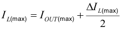
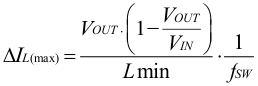
where:
- IL(max) is the maximum inductor current.
- ΔIL(max) is the peak-to-peak inductor ripple current.
- Lmin is the minimum inductance at the operating point.
| TYPE | INDUCTANCE [µH] | CURRENT [A](1) | NOMINAL SWITCHING FREQUENCY | DIMENSIONS [L × W × H] mm | MANUFACTURER(2) |
|---|---|---|---|---|---|
| XEL4020-201ME | 0.20 µH, ±20% | 14 | 2.25 MHz | 4 × 4 × 2.1 | Coilcraft |
| XGL4020-251ME | 0.25 µH, ±20% | 12 | 2.25 MHz | 4 × 4 × 2.1 | Coilcraft |
| XEL4030-201ME | 0.20 µH, ±20% | 17 | 2.25 MHz | 4 × 4 × 3.2 | Coilcraft |
Calculating the maximum inductor current using the actual operating conditions gives the minimum saturation current of the inductor needed. A margin of about 20% is recommended to add. A larger inductor value is also useful to get lower ripple current, but increases the transient response time and size as well.