SLUSEC8B March 2021 – April 2024 TPS628501 , TPS628502 , TPS628503
PRODUCTION DATA
- 1
- 1 Features
- 2 Applications
- 3 Description
- 4 Device Comparison Table
- 5 Pin Configuration and Functions
- 6 Specifications
- 7 Parameter Measurement Information
-
8 Detailed Description
- 8.1 Overview
- 8.2 Functional Block Diagram
- 8.3 Feature Description
- 8.4
Device Functional Modes
- 8.4.1 Pulse Width Modulation (PWM) Operation
- 8.4.2 Power Save Mode Operation (PWM/PFM)
- 8.4.3 100% Duty-Cycle Operation
- 8.4.4 Current Limit and Short Circuit Protection
- 8.4.5 Foldback Current Limit and Short Circuit Protection
- 8.4.6 Output Discharge
- 8.4.7 Soft Start
- 8.4.8 Input Overvoltage Protection
- 9 Application and Implementation
- 10Device and Documentation Support
- 11Revision History
- 12Mechanical, Packaging, and Orderable Information
Package Options
Mechanical Data (Package|Pins)
- DRL|8
Thermal pad, mechanical data (Package|Pins)
Orderable Information
8.3.2 COMP/FSET
This pin allows to set three different parameters:
- Internal compensation settings for the control loop (two settings available)
- The switching frequency in PWM mode from 1.8 MHz to 4 MHz
- Enable/disable spread spectrum clocking (SSC)
A resistor from COMP/FSET to GND changes the compensation as well as the switching frequency. The change in compensation allows the user to adopt the device to different values of output capacitance. The resistor must be placed close to the pin to keep the parasitic capacitance on the pin to a minimum. The compensation setting is sampled at start-up of the converter, so a change in the resistor during operation only has an effect on the switching frequency but not on the compensation.
To save external components, the pin can also be directly tied to VIN or GND to set a pre-defined setting. Do not leave the pin floating.
The switching frequency has to be selected based on the input voltage and the output voltage to meet the specifications for the minimum on-time and minimum off-time.
Example: VIN = 5 V, VOUT = 0.6 V --> duty cycle = 0.6 V / 5 V = 0.12
- --> ton,min = 1 / fs × 0.12
- --> fsw,max = 1 / ton,min × 0.12 = 1 / 0.05 µs × 0.12 = 2.4 MHz
The compensation range has to be chosen based on the minimum capacitance used. The capacitance can be increased from the minimum value as given in Table 8-1, up to the maximum of 200 µF in both compensation ranges. If the capacitance of an output changes during operation, for example, when load switches are used to connect or disconnect parts of the circuitry, the compensation has to be chosen for the minimum capacitance on the output. With large output capacitance, the compensation must be done based on that large capacitance to get the best load transient response. Compensating for large output capacitance but placing less capacitance on the output can lead to instability.
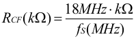
The switching frequency for the different compensation setting is determined by the following equations.
For compensation (comp) setting 1 with spread spectrum clocking (SSC) disabled:
For compensation (comp) setting 1 with spread spectrum clocking (SSC) enabled:
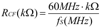
For compensation (comp) setting 2 with spread spectrum clocking (SSC) disabled:

| RCF | COMPENSATION | SWITCHING FREQUENCY | MINIMUM OUTPUT CAPACITANCE FOR VOUT < 1 V | MINIMUM OUTPUT CAPACITANCE FOR 1 V ≤ VOUT < 3.3 V | MINIMUM OUTPUT CAPACITANCE FOR VOUT ≥ 3.3 V |
|---|---|---|---|---|---|
| 10 kΩ .. 4.5 kΩ | for smallest output capacitance (comp setting 1) SSC disabled | 1.8 MHz (10 kΩ) .. 4 MHz (4.5 kΩ) according to Equation 1 | 15 µF | 10 µF | 8 µF |
| 33 kΩ .. 15 kΩ | for smallest output capacitance (comp setting 1) SSC enabled | 1.8 MHz (33 kΩ) .. 4 MHz (15 kΩ) according to Equation 2 | 15 µF | 10 µF | 8 µF |
| 100 kΩ .. 45 kΩ | for best transient response (larger output capacitance) (comp setting 2) SSC disabled | 1.8 MHz (100 kΩ) ..4 MHz (45 kΩ) according to Equation 3 | 30 µF | 18 µF | 15 µF |
| tied to GND | for smallest output capacitance (comp setting 1) SSC disabled | internally fixed 2.25 MHz | 15 µF | 10 µF | 8 µF |
| tied to VIN | for best transient response (larger output capacitance) (comp setting 2) SSC enabled | internally fixed 2.25 MHz | 30 µF | 18 µF | 15 µF |
Refer to Section 9.1.3.2 for further details on the output capacitance required depending on the output voltage.
A resistor value that is too high for RCF is decoded as "tied to VIN". A value below the lowest range is decoded as "tied to GND". The minimum output capacitance in Table 8-1 is for capacitors close to the output of the device. If the capacitance is distributed, a lower compensation setting can be required.