SLUSDO4B August 2020 – June 2022 TPS628510 , TPS628511 , TPS628512 , TPS628513
PRODUCTION DATA
- 1 Features
- 2 Applications
- 3 Description
- 4 Revision History
- 5 Device Comparison Table
- 6 Pin Configuration and Functions
- 7 Specifications
- 8 Parameter Measurement Information
-
9 Detailed Description
- 9.1 Overview
- 9.2 Functional Block Diagram
- 9.3 Feature Description
- 9.4
Device Functional Modes
- 9.4.1 Pulse Width Modulation (PWM) Operation
- 9.4.2 Power Save Mode Operation (PWM/PFM)
- 9.4.3 100% Duty-Cycle Operation
- 9.4.4 Current Limit and Short Circuit Protection
- 9.4.5 Foldback Current Limit and Short Circuit Protection
- 9.4.6 Output Discharge
- 9.4.7 Soft Start / Tracking (SS/TR)
- 9.4.8 Input Overvoltage Protection
- 10Application and Implementation
- 11Power Supply Recommendations
- 12Layout
- 13Device and Documentation Support
- 14Mechanical, Packaging, and Orderable Information
Package Options
Mechanical Data (Package|Pins)
- DRL|8
Thermal pad, mechanical data (Package|Pins)
Orderable Information
9.4.7 Soft Start / Tracking (SS/TR)
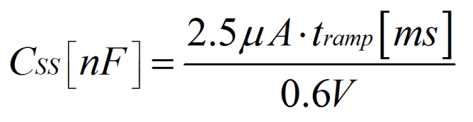
The internal soft-start circuitry controls the output voltage slope during start-up. This avoids excessive inrush current and ensures a controlled output voltage rise time. It also prevents unwanted voltage drops from high impedance power sources or batteries. When EN is set high to start operation, the device starts switching after a delay of about 200 μs, then the internal reference and hence VOUT rises with a slope controlled by an external capacitor connected to the SS/TR pin.
Leaving the SS/TR pin un-connected provides the fastest start-up ramp with 160 µs typically. A capacitor connected from SS/TR to GND is charged with 2.5 µA by an internal current source during soft start until it reaches the reference voltage of 0.6 V. The capacitance required to set a certain ramp-time (tramp) therefore is:
If the device is set to shutdown (EN = GND), undervoltage lockout, or thermal shutdown, an internal resistor pulls the SS/TR pin to GND to ensure a proper low level. Returning from those states causes a new start-up sequence.
A voltage applied at SS/TR can be used to track a master voltage. The output voltage follows this voltage in both directions up and down in forced PWM mode. In PFM mode, the output voltage decreases based on the load current. The SS/TR pin must not be connected to the SS/TR pin of other devices. The maximum value for CSS is 47 nF to ensure proper discharge before the device starts to ramp the output voltage.