SLUSDO4B August 2020 – June 2022 TPS628510 , TPS628511 , TPS628512 , TPS628513
PRODUCTION DATA
- 1 Features
- 2 Applications
- 3 Description
- 4 Revision History
- 5 Device Comparison Table
- 6 Pin Configuration and Functions
- 7 Specifications
- 8 Parameter Measurement Information
-
9 Detailed Description
- 9.1 Overview
- 9.2 Functional Block Diagram
- 9.3 Feature Description
- 9.4
Device Functional Modes
- 9.4.1 Pulse Width Modulation (PWM) Operation
- 9.4.2 Power Save Mode Operation (PWM/PFM)
- 9.4.3 100% Duty-Cycle Operation
- 9.4.4 Current Limit and Short Circuit Protection
- 9.4.5 Foldback Current Limit and Short Circuit Protection
- 9.4.6 Output Discharge
- 9.4.7 Soft Start / Tracking (SS/TR)
- 9.4.8 Input Overvoltage Protection
- 10Application and Implementation
- 11Power Supply Recommendations
- 12Layout
- 13Device and Documentation Support
- 14Mechanical, Packaging, and Orderable Information
Package Options
Mechanical Data (Package|Pins)
- DRL|8
Thermal pad, mechanical data (Package|Pins)
Orderable Information
3 Description
The TPS62851x is a family of pin-to-pin 0.5-A, 1-A, 2-A (continuous), and 3-A (peak) high efficiency, easy-to-use, synchronous step-down DC/DC converters. They are based on a peak current mode control topology. Low resistive switches allow up to 2-A continuous output current and 3-A peak current. The switching frequency is internally fixed at 2.25 MHz and can also be synchronized to an external clock in the range from 1.8 MHz to 4 MHz. In PWM/PFM mode, the TPS62851x automatically enters power save mode at light loads to maintain high efficiency across the whole load range. The TPS62851x provide a 1% output voltage accuracy in PWM mode, which helps design a power supply with high output voltage accuracy. The SS/TR pin allows setting the start-up time or tracking the output voltage to an external source, which allows external sequencing of different supply rails and limits the inrush current during start-up.
The TPS62851xis available in an 8-pin 1.60-mm × 2.10-mm SOT583 package, offering a high power density solution.
| PART NUMBER | PACKAGE(1) | BODY SIZE (NOM) |
|---|---|---|
| TPS628510 | SOT583 | 1.60 mm × 2.10 mm (including pins) |
| TPS628511 | ||
| TPS628512 | ||
| TPS628513 |
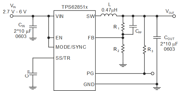
 Simplified Schematic
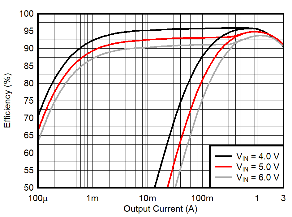
 Efficiency Versus IOUT, VOUT = 3.3 V