SLUSDO4B August 2020 – June 2022 TPS628510 , TPS628511 , TPS628512 , TPS628513
PRODUCTION DATA
- 1 Features
- 2 Applications
- 3 Description
- 4 Revision History
- 5 Device Comparison Table
- 6 Pin Configuration and Functions
- 7 Specifications
- 8 Parameter Measurement Information
-
9 Detailed Description
- 9.1 Overview
- 9.2 Functional Block Diagram
- 9.3 Feature Description
- 9.4
Device Functional Modes
- 9.4.1 Pulse Width Modulation (PWM) Operation
- 9.4.2 Power Save Mode Operation (PWM/PFM)
- 9.4.3 100% Duty-Cycle Operation
- 9.4.4 Current Limit and Short Circuit Protection
- 9.4.5 Foldback Current Limit and Short Circuit Protection
- 9.4.6 Output Discharge
- 9.4.7 Soft Start / Tracking (SS/TR)
- 9.4.8 Input Overvoltage Protection
- 10Application and Implementation
- 11Power Supply Recommendations
- 12Layout
- 13Device and Documentation Support
- 14Mechanical, Packaging, and Orderable Information
Package Options
Mechanical Data (Package|Pins)
- DRL|8
Thermal pad, mechanical data (Package|Pins)
Orderable Information
10.1.2 Inductor Selection
The TPS62851x is designed for a nominal 0.47-µH inductor with a switching frequency of typically 2.25 MHz. Larger values can be used to achieve a lower inductor current ripple but they can have a negative impact on efficiency and transient response. Smaller values than 0.47 µH cause a larger inductor current ripple which causes larger negative inductor current in forced PWM mode at low or no output current. For a higher or lower nominal switching frequency, the inductance must be changed accordingly. See Section 7.3 for details.
The inductor selection is affected by several effects like inductor ripple current, output ripple voltage, PWM-to-PFM transition point, and efficiency. In addition, the inductor selected has to be rated for appropriate saturation current and DC resistance (DCR). Equation 5 calculates the maximum inductor current.
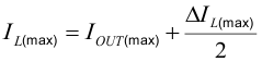
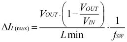
where
- IL(max) is the maximum inductor current
- ΔIL(max) is the peak-to-peak inductor ripple current
- Lmin is the minimum inductance at the operating point
| TYPE | INDUCTANCE [µH] | CURRENT [A](1) | FOR DEVICE | NOMINAL SWITCHING FREQUENCY | DIMENSIONS [LxBxH] mm | MANUFACTURER(2) |
|---|---|---|---|---|---|---|
|
DFE201210U-R47M |
0.47 µH, ±20% | see data sheet | TPS628510/511 / 512 | 2.25 MHz | 2.0 x 1.2 x 1.0 | Murata |
| DFE201210U-1R0M | 1 µH, ±20% | see data sheet | TPS628510/511 / 512 | 2.25 MHz | 2.0x 1.2 x 1.0 |
Murata |
|
DFE201210U-R68 |
0.68 µH, ±20% | see data sheet | TPS628510/511 / 512 | 2.25 MHz | 2.0x 1.2 x 1.0 | Murata |
| XEL3515-561ME | 0.56 µH, ±20% | 4.5 | TPS628510/511 / 512 | 2.25 MHz | 3.5 x 3.2 x 1.5 | Coilcraft |
| XFL4015-701ME | 0.70 µH, ±20% |
3.3 |
TPS628510/511 / 512 | 2.25 MHz | 4.0 x 4.0 x 1.6 | Coilcraft |
| XFL4015-471ME | 0.47 µH, ±20% | 3.5 | TPS628510/511 / 512 | 2.25 MHz | 4.0 x 4.0 x 1.6 | Coilcraft |
Calculating the maximum inductor current using the actual operating conditions gives the minimum saturation current of the inductor needed. A margin of about 20% is recommended to add. A larger inductor value is also useful to get lower ripple current, but increases the transient response time and size as well.