SLVSFS3B September   2020  – July 2021 TPS62868 , TPS62869

PRODUCTION DATA  

  1. Features
  2. Applications
  3. Description
  4. Revision History
  5. Device Options
  6. Pin Configuration and Functions
  7. Specifications
    1. 7.1 Absolute Maximum Ratings
    2. 7.2 ESD Ratings
    3. 7.3 Recommended Operating Conditions
    4. 7.4 Thermal Information
    5. 7.5 Electrical Characteristics
    6. 7.6 I2C InterfaceTiming Characteristics
    7. 7.7 Typical Characteristics
  8. Detailed Description
    1. 8.1 Overview
    2. 8.2 Functional Block Diagram
    3. 8.3 Feature Description
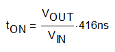
      1. 8.3.1 Power Save Mode
      2. 8.3.2 Forced PWM Mode
      3. 8.3.3 100% Duty Cycle Mode Operation
      4. 8.3.4 Start-up
      5. 8.3.5 Switch Current Limit and HICCUP Short-Circuit Protection
      6. 8.3.6 Undervoltage Lockout (UVLO)
      7. 8.3.7 Thermal Warning and Shutdown
    4. 8.4 Device Functional Modes
      1. 8.4.1 Enable and Disable (EN)
      2. 8.4.2 Output Discharge
      3. 8.4.3 Start-Up Output Voltage and I2C Target Address Selection
        1. 8.4.3.1 TPS6286xxA Devices
        2. 8.4.3.2 TPS6286xxxC Devices
      4. 8.4.4 Select Output Voltage Registers (VID)
      5. 8.4.5 Power Good ( PG)
    5. 8.5 Programming
      1. 8.5.1 Serial Interface Description
      2. 8.5.2 Standard-, Fast-, and Fast-Mode Plus Protocol
      3. 8.5.3 HS-Mode Protocol
      4. 8.5.4 I2C Update Sequence
      5. 8.5.5 I2C Register Reset
    6. 8.6 Register Map
      1. 8.6.1 Target Address Byte
      2. 8.6.2 Register Address Byte
      3. 8.6.3 VOUT Register 1
      4. 8.6.4 VOUT Register 2
      5. 8.6.5 CONTROL Register
      6. 8.6.6 STATUS Register
  9. Application and Implementation
    1. 9.1 Application Information
    2. 9.2 Typical Application
      1. 9.2.1 Design Requirements
      2. 9.2.2 Detailed Design Procedure
        1. 9.2.2.1 Setting The Output Voltage
        2. 9.2.2.2 Output Filter Design
        3. 9.2.2.3 Inductor Selection
        4. 9.2.2.4 Capacitor Selection
      3. 9.2.3 Application Curves
    3. 9.3 Typical Application – TPS6286x0A and TPS6286x0xC Devices
      1. 9.3.1 Design Requirements
      2. 9.3.2 Detailed Design Procedure
        1. 9.3.2.1 Setting the Output Voltage
        2. 9.3.2.2 Output Filter Design
        3. 9.3.2.3 Inductor Selection
        4. 9.3.2.4 Capacitor Selection
      3. 9.3.3 Application Curves
  10. 10Power Supply Recommendations
  11. 11Layout
    1. 11.1 Layout Guidelines
    2. 11.2 Layout Example
      1. 11.2.1 Thermal Considerations
  12. 12Device and Documentation Support
    1. 12.1 Device Support
      1. 12.1.1 Third-Party Products Disclaimer
    2. 12.2 Documentation Support
      1. 12.2.1 Related Documentation
    3. 12.3 Support Resources
    4. 12.4 Receiving Notification of Documentation Updates
    5. 12.5 Trademarks
    6. 12.6 Glossary
    7. 12.7 Electrostatic Discharge Caution
  13. 13Mechanical, Packaging, and Orderable Information

Package Options

Mechanical Data (Package|Pins)
Thermal pad, mechanical data (Package|Pins)
Orderable Information

Power Save Mode

As the load current decreases, the device enters Power Save Mode (PSM) operation. PSM occurs when the inductor current becomes discontinuous, which is when it reaches 0 A during a switching cycle. Power Save Mode is based on a fixed on-time architecture, as shown in Equation 1.

Equation 1. GUID-5E8DE7C8-2673-4E84-9FBA-2E70D9362E85-low.gif

In Power Save Mode, the output voltage rises slightly above the nominal output voltage. This effect is minimized by increasing the output capacitor or inductor value.

When VIN decreases to typically 15% above the VOUT, the TPS6286x does not enter Power Save Mode, regardless of the load current. The device maintains output regulation in PWM mode.