SLVSFM1A March 2021 – November 2023 TPS62902
PRODUCTION DATA
- 1
- 1 Features
- 2 Applications
- 3 Description
- 4 Revision History
- 5 Pin Configuration and Functions
- 6 Specifications
-
7 Detailed Description
- 7.1 Overview
- 7.2 Functional Block Diagram
- 7.3
Feature Description
- 7.3.1 Mode Selection and Device Configuration MODE/S-CONF
- 7.3.2 Adjustable VO Operation (External Voltage Divider)
- 7.3.3 Setable VO Operation (VSET and Internal Voltage Divider)
- 7.3.4 Soft Start / Tracking (SS/TR)
- 7.3.5 Smart Enable with Precise Threshold
- 7.3.6 Power Good (PG)
- 7.3.7 Undervoltage Lockout (UVLO)
- 7.3.8 Current Limit And Short Circuit Protection
- 7.3.9 Thermal Shutdown
- 7.4 Device Functional Modes
-
8 Application and Implementation
- 8.1 Application Information
- 8.2
Typical Application with Adjustable Output Voltage
- 8.2.1 Design Requirements
- 8.2.2 Detailed Design Procedure
- 8.2.3 Application Curves
- 8.2.4 Typical Application with Setable VO using VSET
- 8.3 System Examples
- 8.4 Power Supply Recommendations
- 8.5 Layout
- 9 Device and Documentation Support
- 10Mechanical, Packaging, and Orderable Information
Package Options
Mechanical Data (Package|Pins)
- RPJ|9
Thermal pad, mechanical data (Package|Pins)
Orderable Information
7.4.2 AEE (Automatic Efficiency Enhancement)
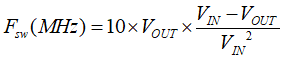
When the MODE/S-CONF pin is configured for AEE mode, the TPS62902 provides the highest efficiency over the entire input voltage and output voltage range by automatically adjusting the switching frequency of the converter. This is achieved by setting the predictive off-time of the converter. The efficiency of a switched mode converter is determined by the power losses during the conversion. The efficiency decreases if VOUT decreases, VIN increases as shown in Equation 4, or both. In order to keep the efficiency high over the entire duty cycle range (VOUT/VIN ratio), the switching frequency is adjusted while maintaining the ripple current.
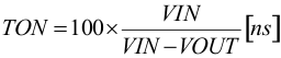
The AEE function in the TPS62902 adjusts the on-time (TON) in power save mode, depending on the input voltage and the output voltage to maintain highest efficiency. The on-time in steady-state operation can be estimated as using Equation 5:
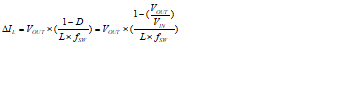
Equation 6 shows the relation among the inductor ripple current, switching frequency, and duty cycle.
Efficiency increases by decreasing switching losses and preserving high efficiency for varying duty cycles, while the ripple current amplitude remains low enough to deliver the full output current without reaching current limit. The AEE feature provides an efficiency enhancement for various duty cycles, especially for lower VOUT values where fixed frequency converters suffer from a significant efficiency drop. Furthermore, this feature compensates for the very small duty cycles of high VIN to low VOUT conversion, which limits the control range in other topologies.