SLVSFM1A March 2021 – November 2023 TPS62902
PRODUCTION DATA
- 1
- 1 Features
- 2 Applications
- 3 Description
- 4 Revision History
- 5 Pin Configuration and Functions
- 6 Specifications
-
7 Detailed Description
- 7.1 Overview
- 7.2 Functional Block Diagram
- 7.3
Feature Description
- 7.3.1 Mode Selection and Device Configuration MODE/S-CONF
- 7.3.2 Adjustable VO Operation (External Voltage Divider)
- 7.3.3 Setable VO Operation (VSET and Internal Voltage Divider)
- 7.3.4 Soft Start / Tracking (SS/TR)
- 7.3.5 Smart Enable with Precise Threshold
- 7.3.6 Power Good (PG)
- 7.3.7 Undervoltage Lockout (UVLO)
- 7.3.8 Current Limit And Short Circuit Protection
- 7.3.9 Thermal Shutdown
- 7.4 Device Functional Modes
-
8 Application and Implementation
- 8.1 Application Information
- 8.2
Typical Application with Adjustable Output Voltage
- 8.2.1 Design Requirements
- 8.2.2 Detailed Design Procedure
- 8.2.3 Application Curves
- 8.2.4 Typical Application with Setable VO using VSET
- 8.3 System Examples
- 8.4 Power Supply Recommendations
- 8.5 Layout
- 9 Device and Documentation Support
- 10Mechanical, Packaging, and Orderable Information
Package Options
Mechanical Data (Package|Pins)
- RPJ|9
Thermal pad, mechanical data (Package|Pins)
Orderable Information
8.2.2.6 Tracking Function
If a tracking function is desired, the SS/TR pin can be used for this purpose by connecting it to an external tracking voltage. The output voltage tracks that voltage with the typical gain and offset as specified in the Electrical Characteristics.
 Figure 8-5 Tracking
Operation Simplified Schematic
Figure 8-5 Tracking
Operation Simplified Schematic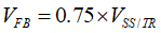
When the SS/TR pin voltage is above 0.8 V, the internal voltage is clamped and the device goes to normal regulation. This works for rising and falling tracking voltages with the same behavior, as long as the input voltage is inside the recommended operating conditions. For decreasing SS/TR pin voltage in PFM mode, the device does not sink current from the output. The resulting decrease of the output voltage can therefore be slower than the SS/TR pin voltage if the load is light. When driving the SS/TR pin with an external voltage, do not exceed the voltage rating of the SS/TR pin, which is 6 V. The SS/TR pin is internally connected with a resistor to GND when EN = 0.
If the input voltage drops below undervoltage lockout, the output voltage goes to zero, independent of the tracking voltage. Figure 8-6 shows how to connect devices to get ratiometric and simultaneous sequencing by using the tracking function. See Section 8.3.3 in the systems examples.
 Figure 8-6 Schematic for Ratiometric and
Simultaneous Start-up
Figure 8-6 Schematic for Ratiometric and
Simultaneous Start-upThe resistive divider of R7 and R8 can be used to change the ramp rate of VOUT2 to be faster, slower, or the same as VOUT1.
A sequential start-up is achieved by connecting the PG pin of VOUT of device 1 to the EN pin of device 2. PG requires a pullup resistor. Ratiometric start-up sequence happens if both supplies are sharing the same soft-start capacitor. Equation 14 gives the soft-start time, though the SS/TR current has to be doubled. Details about these and other tracking and sequencing circuits are found in SLVA470.
If the voltage at the FB pin is below its typical value of 0.6 V, the output voltage accuracy can have a wider tolerance than specified. The current of 2.5 µA out of the SS/TR pin also has an influence on the tracking function, especially for high resistive external voltage dividers on the SS/TR pin.