SLVSES3A February 2021 – March 2021 TPS62903
PRODUCTION DATA
- 1 Features
- 2 Applications
- 3 Description
- 4 Revision History
- 5 Pin Configuration and Functions
- 6 Specifications
-
7 Detailed Description
- 7.1 Overview
- 7.2 Functional Block Diagram
- 7.3
Feature Description
- 7.3.1 Mode Selection and Device Configuration MODE/S-CONF
- 7.3.2 Adjustable VO Operation (External Voltage Divider)
- 7.3.3 Setable VO Operation (VSET and Internal Voltage Divider)
- 7.3.4 Soft Start / Tracking (SS/TR)
- 7.3.5 Smart Enable with Precise Threshold
- 7.3.6 Power Good (PG)
- 7.3.7 Undervoltage Lockout (UVLO)
- 7.3.8 Current Limit And Short Circuit Protection
- 7.3.9 Thermal Shutdown
- 7.4 Device Functional Modes
-
8 Application and Implementation
- 8.1 Application Information
- 8.2
Typical Application with Adjustable Output Voltage
- 8.2.1 Design Requirements
- 8.2.2 Detailed Design Procedure
- 8.2.3 Application Curves
- 8.2.4 Typical Application with Setable VO using VSET
- 8.3 System Examples
- 9 Power Supply Recommendations
- 10Layout
- 11Device and Documentation Support
- 12Mechanical, Packaging, and Orderable Information
Package Options
Mechanical Data (Package|Pins)
- RPJ|9
Thermal pad, mechanical data (Package|Pins)
Orderable Information
8.2.2.4 Inductor Selection
The TPS62903 is designed for a nominal 1-µH inductor. Larger values can be used to achieve a lower inductor current ripple but they can have a negative impact on efficiency and transient response. Smaller values than 1 µH will cause a larger inductor current ripple which causes larger negative inductor current in forced PWM mode at low or no output current. Therefore, they are not recommended at large voltages across the inductor as it is the case for high input voltages and low output voltages. Low-output current in forced PWM mode causes a larger negative inductor current peak which can exceed the negative current limit. At low or no output current and small inductor values, the output voltage cannot be regulated any more. More detailed information on further LC combinations can be found in SLVA463.
The inductor selection is affected by several factors like inductor ripple current, output ripple voltage, PWM-to-PFM transition point, and efficiency. In addition, the inductor selected has to be rated for appropriate saturation current and DC resistance (DCR). Equation 11 calculates the maximum inductor current.
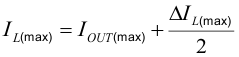
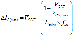
where
- IL(max) is the maximum inductor current
- ΔIL(max) is the maximum peak-to-peak inductor ripple current
- L(min) is the minimum effective inductor value
- fsw is the the actual PWM switching frequency
- VOUT is the output voltage
- VIN(max) is the maximum expected output voltage
Calculating the maximum inductor current using the actual operating conditions gives the needed minimum saturation current of the inductor. It is recommended to add a margin of about 20%. A larger inductor value is also useful to get lower ripple current, but increases the transient response time and size as well. The following inductors have been used with the TPS62903 and are recommended for use:
| TYPE | INDUCTANCE [µH] | CURRENT [A](1) | DIMENSIONS [LxBxH] mm | MANUFACTURER |
|---|---|---|---|---|
| XGL4020-102ME | 1.0 µH, ±20% | 8.8 | 4.0x4.0x2.1 | Coilcraft |
| DFE252012F-1R0M | 1.0 µH, ±20% | 4.7 | 2.5x2.5x1.2 | muRata |
| CIGT252010TM1R0MLE | 1.0 µH, ±20% | 5.3 | 2.5x2.5x1.0 | Samsung |
| TFM252010ALM-1R0MTAA | 1.0 µH, ±20% | 4.7 | 2.5x2.0x1.0 | TDK |
| XEL5030-222ME | 2.2 μH, ±20% | 9.7 | 5.3x5.5x3.1 | Coilcraft |
| XGL4020-222ME | 2.2 μH, ±20% | 6.2 | 4.0x4.0x2.1 | Coilcraft |
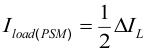
The inductor value also determines the load current at which power save mode is entered: