SLVSES3A February   2021  – March 2021 TPS62903

PRODUCTION DATA  

  1. Features
  2. Applications
  3. Description
  4. Revision History
  5. Pin Configuration and Functions
  6. Specifications
    1. 6.1 Absolute Maximum Ratings
    2. 6.2 ESD Ratings
    3. 6.3 Recommended Operating Conditions
    4. 6.4 Thermal Information
    5. 6.5 Electrical Characteristics
    6. 6.6 Typical Characteristics
  7. Detailed Description
    1. 7.1 Overview
    2. 7.2 Functional Block Diagram
    3. 7.3 Feature Description
      1. 7.3.1 Mode Selection and Device Configuration MODE/S-CONF
      2. 7.3.2 Adjustable VO Operation (External Voltage Divider)
      3. 7.3.3 Setable VO Operation (VSET and Internal Voltage Divider)
      4. 7.3.4 Soft Start / Tracking (SS/TR)
      5. 7.3.5 Smart Enable with Precise Threshold
      6. 7.3.6 Power Good (PG)
      7. 7.3.7 Undervoltage Lockout (UVLO)
      8. 7.3.8 Current Limit And Short Circuit Protection
      9. 7.3.9 Thermal Shutdown
    4. 7.4 Device Functional Modes
      1. 7.4.1 Pulse Width Modulation (PWM) Operation
      2. 7.4.2 AEE (Automatic Efficiency Enhancement)
      3. 7.4.3 Power Save Mode Operation (Auto PFM/PWM)
      4. 7.4.4 100% Duty-Cycle Operation
      5. 7.4.5 Output Discharge Function
      6. 7.4.6 Starting into a Pre-Biased Load
  8. Application and Implementation
    1. 8.1 Application Information
    2. 8.2 Typical Application with Adjustable Output Voltage
      1. 8.2.1 Design Requirements
      2. 8.2.2 Detailed Design Procedure
        1. 8.2.2.1 Custom Design With WEBENCH® Tools
        2. 8.2.2.2 Programming the Output Voltage
        3. 8.2.2.3 External Component Selection
        4. 8.2.2.4 Inductor Selection
        5. 8.2.2.5 Capacitor Selection
          1. 8.2.2.5.1 Output Capacitor
          2. 8.2.2.5.2 Input Capacitor
          3. 8.2.2.5.3 Soft-Start Capacitor
        6. 8.2.2.6 Tracking Function
        7. 8.2.2.7 Output Filter and Loop Stability
      3. 8.2.3 Application Curves
      4. 8.2.4 Typical Application with Setable VO using VSET
        1. 8.2.4.1 Design Requirements
        2. 8.2.4.2 Detailed Design Procedure
        3. 8.2.4.3 Application Curves
    3. 8.3 System Examples
      1. 8.3.1 LED Power Supply
      2. 8.3.2 Powering Multiple Loads
      3. 8.3.3 Voltage Tracking
  9. Power Supply Recommendations
  10. 10Layout
    1. 10.1 Layout Guidelines
    2. 10.2 Layout Example
      1. 10.2.1 Thermal Considerations
  11. 11Device and Documentation Support
    1. 11.1 Device Support
      1. 11.1.1 Development Support
        1. 11.1.1.1 Custom Design With WEBENCH® Tools
    2. 11.2 Receiving Notification of Documentation Updates
    3. 11.3 Support Resources
    4. 11.4 Trademarks
    5. 11.5 Electrostatic Discharge Caution
    6. 11.6 Glossary
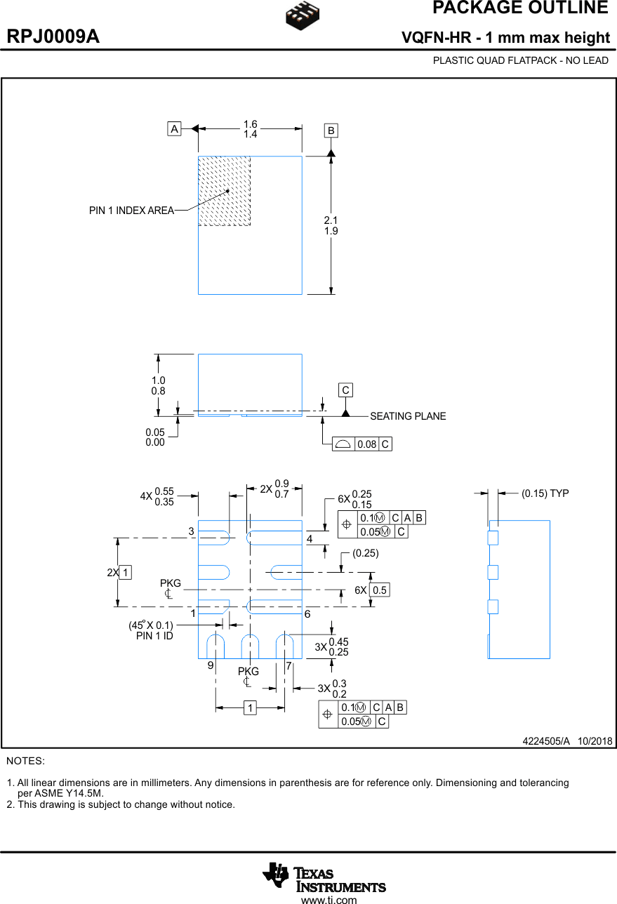
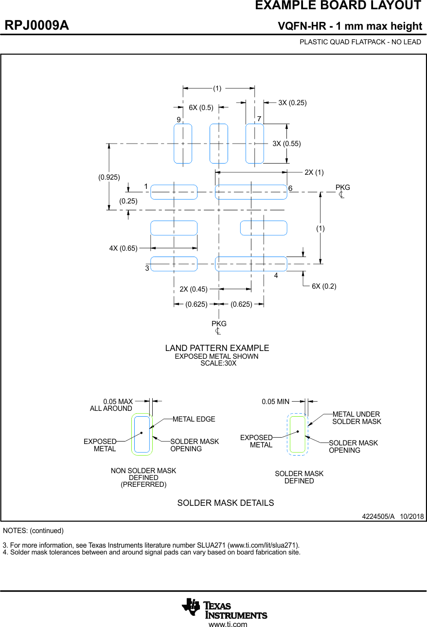
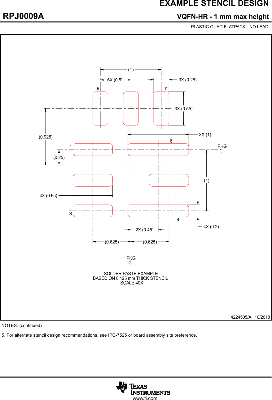
  12. 12Mechanical, Packaging, and Orderable Information

Package Options

Mechanical Data (Package|Pins)
  • RPJ|9
Thermal pad, mechanical data (Package|Pins)
Orderable Information

Mechanical, Packaging, and Orderable Information

The following pages include mechanical, packaging, and orderable information. This information is the most current data available for the designated devices. This data is subject to change without notice and revision of this document. For browser-based versions of this data sheet, refer to the left-hand navigation.

GUID-20210202-CA0I-P0J0-CWMV-7CCVWTDDRTFL-low.gif
GUID-20210202-CA0I-WMNM-TRP4-BWBQMPVDZGMS-low.gif
GUID-20210202-CA0I-ZCTH-ZLHV-NK6GXMQDWTDX-low.gif