SLVSES3A February 2021 – March 2021 TPS62903
PRODUCTION DATA
- 1 Features
- 2 Applications
- 3 Description
- 4 Revision History
- 5 Pin Configuration and Functions
- 6 Specifications
-
7 Detailed Description
- 7.1 Overview
- 7.2 Functional Block Diagram
- 7.3
Feature Description
- 7.3.1 Mode Selection and Device Configuration MODE/S-CONF
- 7.3.2 Adjustable VO Operation (External Voltage Divider)
- 7.3.3 Setable VO Operation (VSET and Internal Voltage Divider)
- 7.3.4 Soft Start / Tracking (SS/TR)
- 7.3.5 Smart Enable with Precise Threshold
- 7.3.6 Power Good (PG)
- 7.3.7 Undervoltage Lockout (UVLO)
- 7.3.8 Current Limit And Short Circuit Protection
- 7.3.9 Thermal Shutdown
- 7.4 Device Functional Modes
-
8 Application and Implementation
- 8.1 Application Information
- 8.2
Typical Application with Adjustable Output Voltage
- 8.2.1 Design Requirements
- 8.2.2 Detailed Design Procedure
- 8.2.3 Application Curves
- 8.2.4 Typical Application with Setable VO using VSET
- 8.3 System Examples
- 9 Power Supply Recommendations
- 10Layout
- 11Device and Documentation Support
- 12Mechanical, Packaging, and Orderable Information
Package Options
Mechanical Data (Package|Pins)
- RPJ|9
Thermal pad, mechanical data (Package|Pins)
Orderable Information
8.2.2.7 Output Filter and Loop Stability
The devices of the TPS62903 family are internally compensated to be stable with L-C filter combinations corresponding to a corner frequency to be calculated with Equation 16:
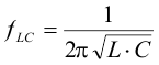
Proven nominal values for inductance and ceramic capacitance are given in Section 8.2.2.3 and are recommended for use. Different values can work, but care has to be taken on the loop stability which is affected. More information including a detailed LC stability matrix can be found in SLVA463.
The TPS62903 devices include an internal 3-pF feedforward capacitor, connected between the VOS and FB pins. This capacitor impacts the frequency behavior and sets a pole and zero in the control loop with the resistors of the feedback divider, per Equation 17 and Equation 18:
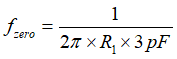
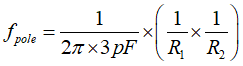
Though the TPS62903 devices are stable without the pole and zero being in a particular location, adjusting their location to the specific needs of the application can provide better performance in power save mode, improved transient response, or both. An external feedforward capacitor can also be added. A more detailed discussion on the optimization for stability versus transient response can be found in SLVA289 and SLVA466.