SLVSFP4B August 2020 – March 2021 TPS62912 , TPS62913
PRODUCTION DATA
- 1 Features
- 2 Applications
- 3 Description
- 4 Revision History
- 5 Pin Configuration and Functions
- 6 Specifications
-
7 Detailed Description
- 7.1 Overview
- 7.2 Functional Block Diagram
- 7.3
Feature Description
- 7.3.1 Smart Config (S-CONF)
- 7.3.2 Device Enable (EN/SYNC)
- 7.3.3 Device Synchronization (EN/SYNC)
- 7.3.4 Spread Spectrum Modulation
- 7.3.5 Output Discharge
- 7.3.6 Undervoltage Lockout (UVLO)
- 7.3.7 Power-Good Output
- 7.3.8 Noise Reduction and Soft-Start Capacitor (NR/SS)
- 7.3.9 Current Limit and Short Circuit Protection
- 7.3.10 Thermal Shutdown
- 7.4 Device Functional Modes
- 8 Application and Implementation
- 9 Power Supply Recommendations
- 10Layout
- 11Device and Documentation Support
- 12Mechanical, Packaging, and Orderable Information
Package Options
Mechanical Data (Package|Pins)
- RPU|10
Thermal pad, mechanical data (Package|Pins)
Orderable Information
3 Description
The TPS6291x devices are a family of high-efficiency, low noise and low ripple current mode synchronous buck converters. The devices are ideal for noise sensitive applications that would normally use an LDO for post regulation such as high-speed ADCs, clock and jitter cleaner, serializer, de-serializer, and radar applications.
The devices operate at a fixed switching frequency of 2.2 MHz or 1 MHz, and can be synchronized to an external clock.
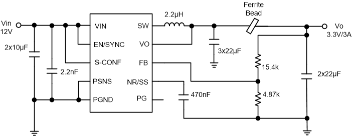
To further reduce the output voltage ripple, the device integrates loop compensation to operate with an optional second-stage ferrite bead L-C filter. This allows an output voltage ripple below 10 µVRMS.
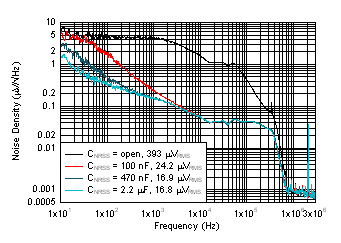
Low-frequency noise levels, similar to a low-noise LDO, are achieved by filtering the internal voltage reference with a capacitor connected to the NR/SS pin.
The optional spread spectrum modulation scheme spreads the DC/DC switching frequency over a wider span, which lowers the mixing spurs.
| DEVICE NAME | OUTPUT CURRENT | PACKAGE(1) | BODY SIZE (NOM) |
|---|---|---|---|
| TPS62912 | 2 A | QFN (10) | 2.0 mm × 2.0 mm |
| TPS62913 | 3 A |
 Output Noise Versus Frequency
 Typical Application