SLVSFP4B August 2020 – March 2021 TPS62912 , TPS62913
PRODUCTION DATA
- 1 Features
- 2 Applications
- 3 Description
- 4 Revision History
- 5 Pin Configuration and Functions
- 6 Specifications
-
7 Detailed Description
- 7.1 Overview
- 7.2 Functional Block Diagram
- 7.3
Feature Description
- 7.3.1 Smart Config (S-CONF)
- 7.3.2 Device Enable (EN/SYNC)
- 7.3.3 Device Synchronization (EN/SYNC)
- 7.3.4 Spread Spectrum Modulation
- 7.3.5 Output Discharge
- 7.3.6 Undervoltage Lockout (UVLO)
- 7.3.7 Power-Good Output
- 7.3.8 Noise Reduction and Soft-Start Capacitor (NR/SS)
- 7.3.9 Current Limit and Short Circuit Protection
- 7.3.10 Thermal Shutdown
- 7.4 Device Functional Modes
- 8 Application and Implementation
- 9 Power Supply Recommendations
- 10Layout
- 11Device and Documentation Support
- 12Mechanical, Packaging, and Orderable Information
Package Options
Mechanical Data (Package|Pins)
- RPU|10
Thermal pad, mechanical data (Package|Pins)
Orderable Information
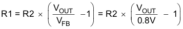
8.2.2.2.6 Setting the Output Voltage
Choose resistors R1 and R2 to set the output voltage within a range of 0.8 V to 5.5 V, according to Equation 8. To keep the feedback network robust from noise, and to reduce the self-generated noise of resistors, set R2 equal to or lower than 5 kΩ. Lower values of FB resistors achieve better noise immunity, and lower light load efficiency, as explained in the Design Considerations for a Resistive Feedback Divider in a DC/DC Converter Technical Brief.
A feedforward capacitor (CFF) is not required for proper operation, but can further improve output noise. However, care must be taken in choosing the CFF, since the power good (PG) function may not be valid with a large CFF during start-up, and can cause spurious triggering of the PG pin during a large load transient. The noise performance with various CFF is shown in Figure 6-31. Refer to the Pros and Cons Using a Feedforward Capacitor with a Low Dropout Regulator Application Report for a discussion of the pros and cons of using a feedforward capacitor.