SLVSFP4B August 2020 – March 2021 TPS62912 , TPS62913
PRODUCTION DATA
- 1 Features
- 2 Applications
- 3 Description
- 4 Revision History
- 5 Pin Configuration and Functions
- 6 Specifications
-
7 Detailed Description
- 7.1 Overview
- 7.2 Functional Block Diagram
- 7.3
Feature Description
- 7.3.1 Smart Config (S-CONF)
- 7.3.2 Device Enable (EN/SYNC)
- 7.3.3 Device Synchronization (EN/SYNC)
- 7.3.4 Spread Spectrum Modulation
- 7.3.5 Output Discharge
- 7.3.6 Undervoltage Lockout (UVLO)
- 7.3.7 Power-Good Output
- 7.3.8 Noise Reduction and Soft-Start Capacitor (NR/SS)
- 7.3.9 Current Limit and Short Circuit Protection
- 7.3.10 Thermal Shutdown
- 7.4 Device Functional Modes
- 8 Application and Implementation
- 9 Power Supply Recommendations
- 10Layout
- 11Device and Documentation Support
- 12Mechanical, Packaging, and Orderable Information
Package Options
Mechanical Data (Package|Pins)
- RPU|10
Thermal pad, mechanical data (Package|Pins)
Orderable Information
7.3.9 Current Limit and Short Circuit Protection
The device is protected against short circuits and overcurrent. The switch current limit prevents the device from high inductor current and from drawing excessive current from the input voltage rail. Excessive current can occur with a shorted/saturated inductor or a heavy load/shorted output circuit condition. If the inductor current reaches the threshold ISWpeak, the high-side MOSFET is turned off and the low-side MOSFET is turned on to ramp down the inductor current. The high-side MOSFET is turned on again only when the low-side current is below the low-side sourcing current limit ISWvalley.
Due to internal propagation delay, the actual current can exceed the static current limit, especially if the input voltage is high and very small inductances are used. The dynamic current limit is calculated as follows:
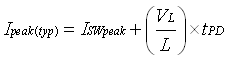
where
- ISWpeak is the static current limit, specified in Section 6.5
- L is the inductance
- VL is the voltage across the inductor (VIN - VOUT)
- tPD is the internal propagation delay, typically 50 ns
The low-side MOSFET also contains a negative current limit to prevent excessive current from flowing back through the inductor to the input. If the low-side sinking current limit is exceeded, the low-side MOSFET is turned off. In this scenario, both MOSFETs are off until the start of the next cycle.