SLVSFW3 March 2022 TPS629203-Q1
PRODUCTION DATA
- 1 Features
- 2 Applications
- 3 Description
- 4 Revision History
- 5 Device Comparison Table
- 6 Pin Configuration and Functions
- 7 Specifications
-
8 Detailed Description
- 8.1 Overview
- 8.2 Functional Block Diagram
- 8.3
Feature Description
- 8.3.1 Mode Selection and Device Configuration (MODE/S-CONF Pin)
- 8.3.2 Adjustable VO Operation (External Voltage Divider)
- 8.3.3 Selectable VO Operation (VSET and Internal Voltage Divider)
- 8.3.4 Smart Enable with Precise Threshold
- 8.3.5 Power Good (PG)
- 8.3.6 Output Discharge Function
- 8.3.7 Undervoltage Lockout (UVLO)
- 8.3.8 Current Limit and Short Circuit Protection
- 8.3.9 Thermal Shutdown
- 8.4 Device Functional Modes
- 9 Application and Implementation
- 10Power Supply Recommendations
- 11Layout
- 12Device and Documentation Support
- 13Mechanical, Packaging, and Orderable Information
Package Options
Mechanical Data (Package|Pins)
- DRL|8
Thermal pad, mechanical data (Package|Pins)
Orderable Information
8.3.8 Current Limit and Short Circuit Protection
The TPS629203-Q1 is protected against overload and short circuit events. If the inductor current exceeds the current limit, ILIM_HS, the high-side switch is turned off and the low-side switch is turned on to ramp down the inductor current. The high-side FET turns on again only if the current in the low-side FET has decreased below the low-side current limit threshold, ILIM_LS.
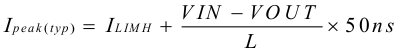
Due to internal propagation delay, the actual current can exceed the static current limit during that time. The dynamic current limit is given in Equation 1.
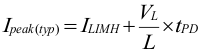
where:
- ILIMH is the static current limit as specified in the electrical characteristics.
- L is the effective inductance at the peak current.
- VL is the voltage across the inductor (VIN – VOUT).
- tPD is the internal propagation delay of typically 50 ns.
The current limit can exceed static values, especially if the input voltage is high and very small inductances are used. The dynamic high-side switch peak current can be calculated as follows:
The TPS629203-Q1 also includes a low-side negative current limit (ILIM:SINK) to protect against excessive negative currents that can occur in forced PMW mode under heavy to light load transient conditions. If the negative current in the low-side switch exceeds the ILIM:SINK threshold, the low-side switch is disabled. Both the low-side and high-side switches remain off until an internal timer re-enables the high-side switch based on the selected PWM switching frequency.