SLVSFW3 March 2022 TPS629203-Q1
PRODUCTION DATA
- 1 Features
- 2 Applications
- 3 Description
- 4 Revision History
- 5 Device Comparison Table
- 6 Pin Configuration and Functions
- 7 Specifications
-
8 Detailed Description
- 8.1 Overview
- 8.2 Functional Block Diagram
- 8.3
Feature Description
- 8.3.1 Mode Selection and Device Configuration (MODE/S-CONF Pin)
- 8.3.2 Adjustable VO Operation (External Voltage Divider)
- 8.3.3 Selectable VO Operation (VSET and Internal Voltage Divider)
- 8.3.4 Smart Enable with Precise Threshold
- 8.3.5 Power Good (PG)
- 8.3.6 Output Discharge Function
- 8.3.7 Undervoltage Lockout (UVLO)
- 8.3.8 Current Limit and Short Circuit Protection
- 8.3.9 Thermal Shutdown
- 8.4 Device Functional Modes
- 9 Application and Implementation
- 10Power Supply Recommendations
- 11Layout
- 12Device and Documentation Support
- 13Mechanical, Packaging, and Orderable Information
Package Options
Mechanical Data (Package|Pins)
- DRL|8
Thermal pad, mechanical data (Package|Pins)
Orderable Information
9.2.2.3.1 Output Filter and Loop Stability
The TPS629203-Q1 is internally compensated to be stable with a range of LC filter combinations. The LC output filters inductance and capacitance have to be considered together, creating a double pole, responsible for the corner frequency of the converter using Equation 13.
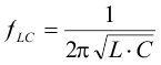
Table 9-3 can be used to simplify the output filter component selection. The values in Table 9-3 are nominal values, and the effective capacitance was considered to be +20% and –50%. Different values can work, but care has to be taken on the loop stability which is affected. More information on the sizing of the LC filter of a DCS-Control regulator can be found in the Optimizing the TPS62130/40/50/60 Output Filter Application Note.
| 4.7 µF | 10 µF | 22 µF | 47 µF | 100 µF | 200 µF | |
|---|---|---|---|---|---|---|
| 1 µH(3)(4) | √ | √ | √ | √(2) | ||
| 1.5 µH | √ | √ | √ | √(2) | ||
| 2.2 µH | √ | √(1) | √ | √(2) | ||
| 3.3 µH | √ | √ | √ | √ | ||
| 4.7 µH | √ | √ | √ | √(2) |
Although the TPS629203-Q1 is stable without the pole and zero being in a particular location, an external feedforward capacitor can also be added to adjust their location based on the specific needs of the application. This can provide better performance in power save mode, improved transient response, or both.
A more detailed discussion on the optimization for stability versus transient response can be found in the Optimizing Transient Response of Internally Compensated DC-DC Converters Application Note and Feedforward Capacitor to Improve Stability and Bandwidth of TPS621/821-Family Application Note.