SLVSGE2 March 2022 TPS629203
PRODUCTION DATA
- 1 Features
- 2 Applications
- 3 Description
- 4 Revision History
- 5 Device Comparison Table
- 6 Pin Configuration and Functions
- 7 Specifications
-
8 Detailed Description
- 8.1 Overview
- 8.2 Functional Block Diagram
- 8.3
Feature Description
- 8.3.1 Mode Selection and Device Configuration (MODE/S-CONF Pin)
- 8.3.2 Adjustable VO Operation (External Voltage Divider)
- 8.3.3 Selectable VO Operation (VSET and Internal Voltage Divider)
- 8.3.4 Smart Enable with Precise Threshold
- 8.3.5 Power Good (PG)
- 8.3.6 Output Discharge Function
- 8.3.7 Undervoltage Lockout (UVLO)
- 8.3.8 Current Limit and Short Circuit Protection
- 8.3.9 Thermal Shutdown
- 8.4 Device Functional Modes
- 9 Application and Implementation
- 10Power Supply Recommendations
- 11Layout
- 12Device and Documentation Support
- 13Mechanical, Packaging, and Orderable Information
Package Options
Mechanical Data (Package|Pins)
- DRL|8
Thermal pad, mechanical data (Package|Pins)
Orderable Information
9.2.2.2 Programming the Output Voltage
The output voltage of the TPS629203 is adjustable. It can be programmed for output voltages from 0.6 V to 5.5 V, using a resistor divider from VOUT to GND. The voltage at the FB pin is regulated to 600 mV. The value of the output voltage is set by the selection of the resistor divider from Table 9-2. It is recommended to choose resistor values that allow a current of at least 2 μA, meaning the value of R2 should not exceed 300 kΩ. Lower resistor values are recommended for highest accuracy and most robust design.
Equation 12. 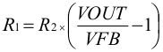
where
- VFB is 0.6 V.
Table 9-2 Setting the Output Voltage
| Nominal Output Voltage | R1 | R2 | Exact Output Voltage |
|---|---|---|---|
| 0.8 V | 51 kΩ | 150 kΩ | 0.804 V |
| 1.2 V | 130 kΩ | 130 kΩ | 1.200 V |
| 1.5 V | 150 kΩ | 100 kΩ | 1.500 V |
| 1.8 V | 475 kΩ | 237 kΩ | 1.803 V |
| 2.5 V | 523 kΩ | 165 kΩ | 2.502 V |
| 3.3 V | 619 kΩ | 137 kΩ | 3.311 V |
| 5 V | 619 kΩ | 84.5 kΩ | 4.995 V |