SLVSGE2 March 2022 TPS629203
PRODUCTION DATA
- 1 Features
- 2 Applications
- 3 Description
- 4 Revision History
- 5 Device Comparison Table
- 6 Pin Configuration and Functions
- 7 Specifications
-
8 Detailed Description
- 8.1 Overview
- 8.2 Functional Block Diagram
- 8.3
Feature Description
- 8.3.1 Mode Selection and Device Configuration (MODE/S-CONF Pin)
- 8.3.2 Adjustable VO Operation (External Voltage Divider)
- 8.3.3 Selectable VO Operation (VSET and Internal Voltage Divider)
- 8.3.4 Smart Enable with Precise Threshold
- 8.3.5 Power Good (PG)
- 8.3.6 Output Discharge Function
- 8.3.7 Undervoltage Lockout (UVLO)
- 8.3.8 Current Limit and Short Circuit Protection
- 8.3.9 Thermal Shutdown
- 8.4 Device Functional Modes
- 9 Application and Implementation
- 10Power Supply Recommendations
- 11Layout
- 12Device and Documentation Support
- 13Mechanical, Packaging, and Orderable Information
Package Options
Mechanical Data (Package|Pins)
- DRL|8
Thermal pad, mechanical data (Package|Pins)
Orderable Information
3 Description
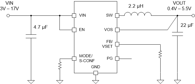
The TPS6292xx family of devices are highly efficient, small, and highly flexible synchronous step-down DC-DC converters that are easy to use. A wide 3-V to 17-V input voltage range supports a wide variety of systems powered from either 12-V, 5-V, or 3.3-V supply rails, or single-cell or multi-cell Li-Ion batteries. The TPS629203 can be configured to run at either 2.5 MHz or 1 MHz in a forced PWM mode or a variable frequency (auto PFM) mode. In auto PFM mode, the device automatically transitions to power save mode at light loads to maintain high efficiency. The low 4-µA typical quiescent current also provides high efficiency down to the smallest loads. TI's automatic efficiency enhancement (AEE) mode holds a high conversion efficiency through the whole operation range without the need of using different inductors by automatically adjusting the switching frequency based on input and output voltages. In addition to selecting the switching frequency behavior, the MODE/S-CONF input pin can also be used to select between different combinations of external and internal feedback dividers and enabling and disabling the output voltage discharge capability. In the internal feedback configuration, a resistor between the FB/VSET pin and GND can be used to select between 18 different output voltage options (see Table 8-2).
| PART NUMBER | PACKAGE(1) | BODY SIZE (NOM) |
|---|---|---|
| TPS629203 | SOT-5X3 (8) | 1.60 mm × 2.10 mm (including pins) |
 Simplified Schematic
VOUT = 3.3 V at 1.0-MHz Auto PFM/PWM