SLUSEA4D June 2021 – August 2022 TPS62932 , TPS62933 , TPS62933F , TPS62933O , TPS62933P
PRODUCTION DATA
- 1 Features
- 2 Applications
- 3 Description
- 4 Revision History
- 5 Description (continued)
- 6 Device Comparison Table
- 7 Pin Configuration and Functions
- 8 Specifications
-
9 Detailed Description
- 9.1 Overview
- 9.2 Functional Block Diagram
- 9.3
Feature Description
- 9.3.1 Fixed Frequency Peak Current Mode
- 9.3.2 Pulse Frequency Modulation
- 9.3.3 Voltage Reference
- 9.3.4 Output Voltage Setting
- 9.3.5 Switching Frequency Selection
- 9.3.6 Enable and Adjusting Undervoltage Lockout
- 9.3.7 External Soft Start and Prebiased Soft Start
- 9.3.8 Power Good
- 9.3.9 Minimum On Time, Minimum Off Time, and Frequency Foldback
- 9.3.10 Frequency Spread Spectrum
- 9.3.11 Overvoltage Protection
- 9.3.12 Overcurrent and Undervoltage Protection
- 9.3.13 Thermal Shutdown
- 9.4 Device Functional Modes
-
10Application and Implementation
- 10.1 Application Information
- 10.2
Typical Application
- 10.2.1 Design Requirements
- 10.2.2
Detailed Design Procedure
- 10.2.2.1 Custom Design With WEBENCH® Tools
- 10.2.2.2 Output Voltage Resistors Selection
- 10.2.2.3 Choosing Switching Frequency
- 10.2.2.4 Soft-Start Capacitor Selection
- 10.2.2.5 Bootstrap Capacitor Selection
- 10.2.2.6 Undervoltage Lockout Setpoint
- 10.2.2.7 Output Inductor Selection
- 10.2.2.8 Output Capacitor Selection
- 10.2.2.9 Input Capacitor Selection
- 10.2.2.10 Feedforward Capacitor CFF Selection
- 10.2.2.11 Maximum Ambient Temperature
- 10.2.3 Application Curves
- 10.3 What to Do and What Not to Do
- 11Power Supply Recommendations
- 12Layout
- 13Device and Documentation Support
- 14Mechanical, Packaging, and Orderable Information
Package Options
Mechanical Data (Package|Pins)
- DRL|8
Thermal pad, mechanical data (Package|Pins)
Orderable Information
10.2.2.11 Maximum Ambient Temperature
As with any power conversion device, the TPS6293x dissipates internal power while operating. The effect of this power dissipation is to raise the internal temperature of the converter above ambient. The internal die temperature (TJ) is a function of the following:
- Ambient temperature
- Power loss
- Effective thermal resistance, RθJA, of the device
- PCB combination
The maximum internal die temperature must be limited to 150°C. This establishes a limit on the maximum device power dissipation and, therefore, the load current. Equation 24 shows the relationships between the important parameters. It is easy to see that larger ambient temperatures (TA) and larger values of RθJA reduce the maximum available output current. The converter efficiency can be estimated by using the curves provided in this data sheet. Note that these curves include the power loss in the inductor. If the desired operating conditions cannot be found in one of the curves, then interpolation can be used to estimate the efficiency. Alternatively, the EVM can be adjusted to match the desired application requirements and the efficiency can be measured directly. The correct value of RθJA is more difficult to estimate. As stated in the Semiconductor and IC Package Thermal Metrics Application Report, the value of RθJA given in the Thermal Information table is not valid for design purposes and must not be used to estimate the thermal performance of the application. The values reported in that table were measured under a specific set of conditions that are rarely obtained in an actual application. The data given for RθJC(bott) and ΨJT can be useful when determining thermal performance. See the Semiconductor and IC Package Thermal Metrics Application Report for more information and the resources given at the end of this section.
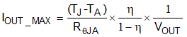
where
- ŋ is efficiency.
The effective RθJA is a critical parameter and depends on many factors such as the following:
- Power dissipation
- Air temperature and flow
- PCB area
- Copper heat-sink area
- Number of thermal vias under the package
- Adjacent component placement