SLUSEA4D June 2021 – August 2022 TPS62932 , TPS62933 , TPS62933F , TPS62933O , TPS62933P
PRODUCTION DATA
- 1 Features
- 2 Applications
- 3 Description
- 4 Revision History
- 5 Description (continued)
- 6 Device Comparison Table
- 7 Pin Configuration and Functions
- 8 Specifications
-
9 Detailed Description
- 9.1 Overview
- 9.2 Functional Block Diagram
- 9.3
Feature Description
- 9.3.1 Fixed Frequency Peak Current Mode
- 9.3.2 Pulse Frequency Modulation
- 9.3.3 Voltage Reference
- 9.3.4 Output Voltage Setting
- 9.3.5 Switching Frequency Selection
- 9.3.6 Enable and Adjusting Undervoltage Lockout
- 9.3.7 External Soft Start and Prebiased Soft Start
- 9.3.8 Power Good
- 9.3.9 Minimum On Time, Minimum Off Time, and Frequency Foldback
- 9.3.10 Frequency Spread Spectrum
- 9.3.11 Overvoltage Protection
- 9.3.12 Overcurrent and Undervoltage Protection
- 9.3.13 Thermal Shutdown
- 9.4 Device Functional Modes
-
10Application and Implementation
- 10.1 Application Information
- 10.2
Typical Application
- 10.2.1 Design Requirements
- 10.2.2
Detailed Design Procedure
- 10.2.2.1 Custom Design With WEBENCH® Tools
- 10.2.2.2 Output Voltage Resistors Selection
- 10.2.2.3 Choosing Switching Frequency
- 10.2.2.4 Soft-Start Capacitor Selection
- 10.2.2.5 Bootstrap Capacitor Selection
- 10.2.2.6 Undervoltage Lockout Setpoint
- 10.2.2.7 Output Inductor Selection
- 10.2.2.8 Output Capacitor Selection
- 10.2.2.9 Input Capacitor Selection
- 10.2.2.10 Feedforward Capacitor CFF Selection
- 10.2.2.11 Maximum Ambient Temperature
- 10.2.3 Application Curves
- 10.3 What to Do and What Not to Do
- 11Power Supply Recommendations
- 12Layout
- 13Device and Documentation Support
- 14Mechanical, Packaging, and Orderable Information
Package Options
Mechanical Data (Package|Pins)
- DRL|8
Thermal pad, mechanical data (Package|Pins)
Orderable Information
10.2.2.9 Input Capacitor Selection
The TPS6293x device requires an input decoupling capacitor and, depending on the application, a bulk input capacitor. The typical recommended value for the decoupling capacitor is 10 μF, and an additional 0.1-µF capacitor from the VIN pin to ground is recommended to provide high frequency filtering.
The value of a ceramic capacitor varies significantly over temperature and the amount of DC bias applied to the capacitor. X5R and X7R ceramic dielectrics are recommended because they have a high capacitance-to-volume ratio and are fairly stable over temperature. The capacitor must also be selected with the DC bias taken into account. The effective capacitance value decreases as the DC bias increases.
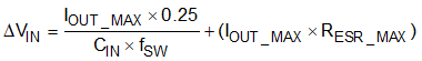
The capacitor voltage rating needs to be greater than the maximum input voltage. The capacitor must also have a ripple current rating greater than the maximum input current ripple. The input ripple current can be calculated using Equation 22.
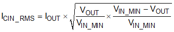
For this example design, two TDK CGA5L1X7R1H106K160AC (10-μF, 50-V, 1206, X7R) capacitors have been selected. The effective capacitance under input voltage of 24 V for each one is 3.45 μF. The input capacitance value determines the input ripple voltage of the converter. The input voltage ripple can be calculated using Equation 23. Using the design example values, IOUT_MAX = 3 A, CIN_EFF = 2 × 3.45 = 6.9 μF, and fSW = 500 kHz, yields an input voltage ripple of 222 mV and a RMS input ripple current of 1.22 A.
where
- RESR_MAX is the maximum series resistance of the input capacitor, which is approximately 1.5 mΩ of two capacitors in paralleled.