SLUSEA4D June 2021 – August 2022 TPS62932 , TPS62933 , TPS62933F , TPS62933O , TPS62933P
PRODUCTION DATA
- 1 Features
- 2 Applications
- 3 Description
- 4 Revision History
- 5 Description (continued)
- 6 Device Comparison Table
- 7 Pin Configuration and Functions
- 8 Specifications
-
9 Detailed Description
- 9.1 Overview
- 9.2 Functional Block Diagram
- 9.3
Feature Description
- 9.3.1 Fixed Frequency Peak Current Mode
- 9.3.2 Pulse Frequency Modulation
- 9.3.3 Voltage Reference
- 9.3.4 Output Voltage Setting
- 9.3.5 Switching Frequency Selection
- 9.3.6 Enable and Adjusting Undervoltage Lockout
- 9.3.7 External Soft Start and Prebiased Soft Start
- 9.3.8 Power Good
- 9.3.9 Minimum On Time, Minimum Off Time, and Frequency Foldback
- 9.3.10 Frequency Spread Spectrum
- 9.3.11 Overvoltage Protection
- 9.3.12 Overcurrent and Undervoltage Protection
- 9.3.13 Thermal Shutdown
- 9.4 Device Functional Modes
-
10Application and Implementation
- 10.1 Application Information
- 10.2
Typical Application
- 10.2.1 Design Requirements
- 10.2.2
Detailed Design Procedure
- 10.2.2.1 Custom Design With WEBENCH® Tools
- 10.2.2.2 Output Voltage Resistors Selection
- 10.2.2.3 Choosing Switching Frequency
- 10.2.2.4 Soft-Start Capacitor Selection
- 10.2.2.5 Bootstrap Capacitor Selection
- 10.2.2.6 Undervoltage Lockout Setpoint
- 10.2.2.7 Output Inductor Selection
- 10.2.2.8 Output Capacitor Selection
- 10.2.2.9 Input Capacitor Selection
- 10.2.2.10 Feedforward Capacitor CFF Selection
- 10.2.2.11 Maximum Ambient Temperature
- 10.2.3 Application Curves
- 10.3 What to Do and What Not to Do
- 11Power Supply Recommendations
- 12Layout
- 13Device and Documentation Support
- 14Mechanical, Packaging, and Orderable Information
Package Options
Mechanical Data (Package|Pins)
- DRL|8
Thermal pad, mechanical data (Package|Pins)
Orderable Information
9.3.7 External Soft Start and Prebiased Soft Start
The SS pin of TPS62932, TPS62933, and TPS62933F are used to minimize inrush current when driving capacitive load. The devices use the lower voltage of the internal voltage reference, VREF, or the SS pin voltage as the reference voltage and regulates the output accordingly. A capacitor on the SS pin to ground implements a soft-start time. The device has an internal pullup current source that charges the external soft-start capacitor. Use Equation 6 to calculate the soft-start time (tSS, 0% to 100%) and soft-start capacitor (CSS).
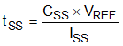
where
- VREF is 0.8 V (the internal reference voltage).
- ISS is 5.5 µA (typical), the internal pullup current.
If the output capacitor is prebiased at start-up, the devices initiate switching and start ramping up only after the internal reference voltage becomes greater than the feedback voltage, VFB. This scheme makes sure that the converters ramp up smoothly into regulation point.
A resistor divider connected to the SS pin can implement voltage tracking of the other power rail.