SLVSGV5A October   2022  – March 2023 TPS62993-Q1

PRODUCTION DATA  

  1. Features
  2. Applications
  3. Description
  4. Revision History
  5. Device Comparison Table
  6. Pin Configuration and Functions
  7. Specifications
    1. 7.1 Absolute Maximum Ratings
    2. 7.2 ESD Ratings
    3. 7.3 Recommended Operating Conditions
    4. 7.4 Thermal Information
    5. 7.5 Electrical Characteristics
    6. 7.6 Typical Characteristics
  8. Detailed Description
    1. 8.1 Overview
    2. 8.2 Functional Block Diagram
    3. 8.3 Feature Description
      1. 8.3.1  Mode Selection and Device Configuration MODE/S-CONF
      2. 8.3.2  Adjustable VO Operation (External Voltage Divider)
      3. 8.3.3  Selectable VO Operation (VSET and Internal Voltage Divider)
      4. 8.3.4  Soft Start and Tracking (SS/TR)
        1. 8.3.4.1 Tracking Function
      5. 8.3.5  Smart Enable with Precise Threshold
      6. 8.3.6  Power Good (PG)
      7. 8.3.7  Output Discharge Function
      8. 8.3.8  Undervoltage Lockout (UVLO)
      9. 8.3.9  Current Limit and Short-Circuit Protection
      10. 8.3.10 High Temperature Specifications
      11. 8.3.11 Thermal Shutdown
    4. 8.4 Device Functional Modes
      1. 8.4.1 Forced Pulse Width Modulation (FPWM) Operation
      2. 8.4.2 Power Save Mode Operation (Auto PFM and PWM)
      3. 8.4.3 AEE (Automatic Efficiency Enhancement)
      4. 8.4.4 100% Duty-Cycle Operation
      5. 8.4.5 Starting into a Prebiased Load
  9. Application and Implementation
    1. 9.1 Application Information
    2. 9.2 Typical Application with Adjustable Output Voltage
      1. 9.2.1 Design Requirements
      2. 9.2.2 Detailed Design Procedure
        1. 9.2.2.1 Custom Design With WEBENCH® Tools
        2. 9.2.2.2 Programming the Output Voltage
        3. 9.2.2.3 External Component Selection
          1. 9.2.2.3.1 Output Filter and Loop Stability
          2. 9.2.2.3.2 Inductor Selection
          3. 9.2.2.3.3 Capacitor Selection
            1. 9.2.2.3.3.1 Output Capacitor
            2. 9.2.2.3.3.2 Input Capacitor
            3. 9.2.2.3.3.3 Soft-Start Capacitor
      3. 9.2.3 Application Curves
        1. 9.2.3.1 Application Curves Vout = 1.8 V
        2. 9.2.3.2 Application Curves Vout = 1.2 V
        3. 9.2.3.3 Application Curves Vout = 0.6 V
    3. 9.3 Typical Application with Selectable VOUT using VSET
      1. 9.3.1 Design Requirements
      2. 9.3.2 Detailed Design Procedure
        1. 9.3.2.1 Programming the Output Voltage
      3. 9.3.3 Application Curves
        1. 9.3.3.1 Application Curves Vout = 5 V
        2. 9.3.3.2 Application Curves Vout = 3.3 V
    4. 9.4 System Examples
      1. 9.4.1 LED Power Supply
      2. 9.4.2 Powering Multiple Loads
      3. 9.4.3 Voltage Tracking
      4. 9.4.4 Inverting Buck-Boost (IBB)
    5. 9.5 Power Supply Recommendations
    6. 9.6 Layout
      1. 9.6.1 Layout Guidelines
      2. 9.6.2 Layout Example
      3. 9.6.3 Thermal Considerations
  10. 10Device and Documentation Support
    1. 10.1 Device Support
      1. 10.1.1 Third-Party Products Disclaimer
      2. 10.1.2 Development Support
        1. 10.1.2.1 Custom Design With WEBENCH® Tools
    2. 10.2 Documentation Support
      1. 10.2.1 Related Documentation
    3. 10.3 Receiving Notification of Documentation Updates
    4. 10.4 Support Resources
    5. 10.5 Trademarks
    6. 10.6 Electrostatic Discharge Caution
    7. 10.7 Glossary
  11. 11Mechanical, Packaging, and Orderable Information

Package Options

Mechanical Data (Package|Pins)
Thermal pad, mechanical data (Package|Pins)
Orderable Information

Application Curves Vout = 3.3 V

GUID-20220812-SS0I-FZ4T-5B0V-LKS2QDJLNN22-low.svg
VOUT = 3.3 V L = 1.0 μH Fsw = 2.5 MHz
Auto PFM/PWM
Figure 9-52 Efficiency vs Output Current
GUID-20220816-SS0I-29NF-BNZ5-V2PDN1QXS3ZR-low.svg
VOUT = 3.3 V L = 1.0 μH Fsw = 2.5 MHz
Auto PFM/PWM
Figure 9-54 Switching Frequency vs Input Voltage
GUID-20220816-SS0I-FJJ1-GKLT-4ZPBST8J4DQS-low.svg
VOUT = 3.3 V L = 1.0 μH Fsw = 2.5 MHz
Auto PFM/PWM
Figure 9-56 Output Voltage vs Output Current
GUID-20220812-SS0I-JT7P-KGSF-R6RK4FWCFC9C-low.svg
VOUT = 3.3 V L = 2.2 μH Fsw = 1.0 MHz
Auto PFM/PWM
Figure 9-58 Efficiency vs Output Current
GUID-20220816-SS0I-F75L-WQWZ-TLWQPFSXDHNR-low.svg
VOUT = 3.3 V L = 2.2 μH Fsw = 1.0 MHz
Auto PFM/PWM
Figure 9-60 Switching Frequency vs Input Voltage
GUID-20220816-SS0I-5VSB-MJ3X-RQ9NMQCJXSFS-low.svg
VOUT = 3.3 V L = 2.2 μH Fsw = 1.0 MHz
Auto PFM/PWM
Figure 9-62 Output Voltage vs Output Current
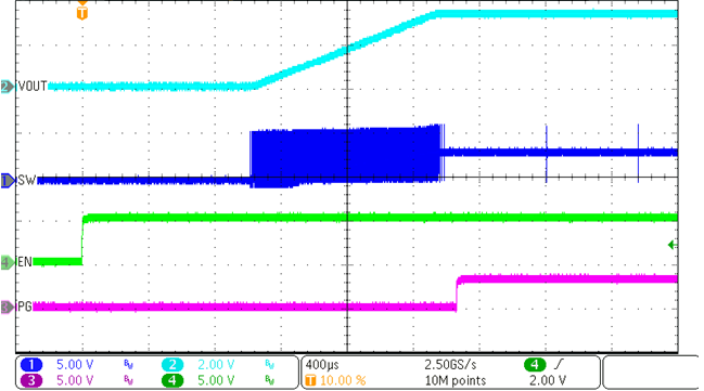
GUID-20221011-SS0I-9NG6-LLZS-XNKFCQB2PBRV-low.png
VIN = 6 V Css = 3.3 nF Fsw = 2.5 MHz
VOUT = 3.3 V IOUT = 0 A Auto PFM/PWM
Figure 9-64 Start-Up Timing
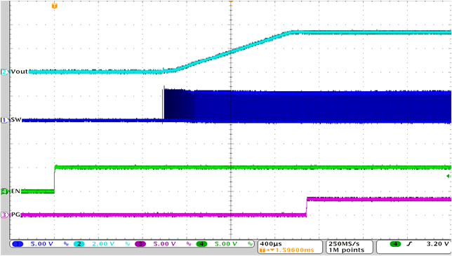
GUID-20221011-SS0I-BTD2-LNJT-GSCFGSDWR1P7-low.png
VIN = 6 V Css = 3.3 nF Fsw = 2.5 MHz
VOUT = 3.3 V IOUT = 3 A FPWM
Figure 9-66 Start-Up Timing
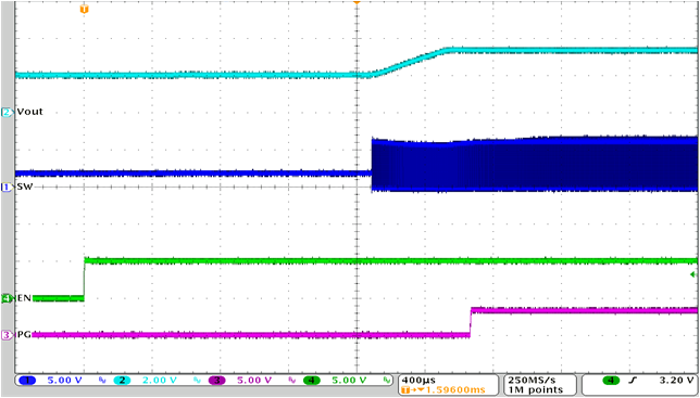
GUID-20221011-SS0I-6KXZ-ZCFV-VMV8ZXP2LJLT-low.png
VIN = 6 V Css = 3.3 nF Fsw = 2.5 MHz
VOUT = 3.3 V IOUT = 0 A FPWM
Figure 9-68 Start-Up into Prebiased Output
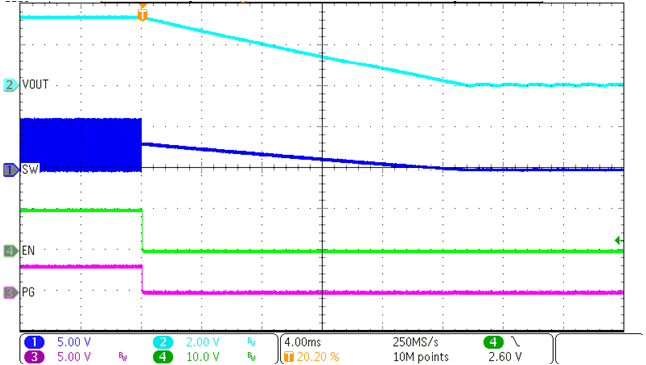
GUID-20221011-SS0I-6HQW-K5DQ-ZHGQTF4VGGDJ-low.png
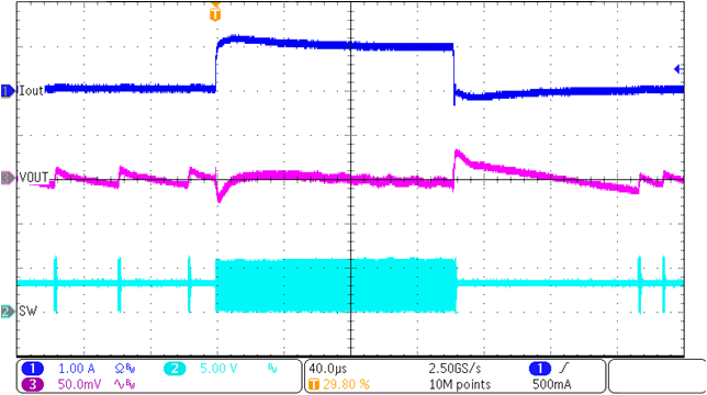
VIN = 6 V L = 1.0 μH Fsw = 2.5 MHz
VOUT = 3.3 V IOUT = 10 mA Auto PFM/PWM
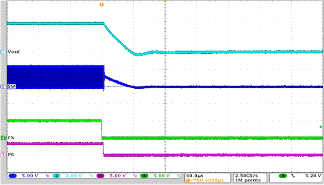
Figure 9-70 Shutdown Timing with Output Discharge Disabled
GUID-20221011-SS0I-FBXG-B8NG-V4HVGHMNLBJB-low.png
VIN = 6 V L = 1.0 μH Fsw = 2.5 MHz
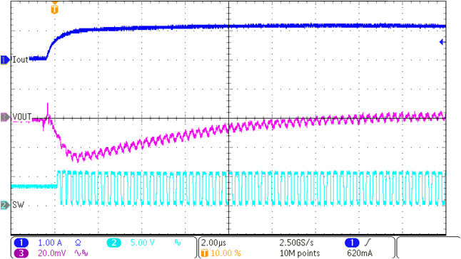
VOUT = 3.3 V IOUT = 10 mA to 1 A Auto PFM/PWM
Figure 9-72 Load Transient Response
GUID-20221011-SS0I-K6VZ-9FH4-NC79FFS6T72N-low.png
VIN = 6 V L = 1.0 μH Fsw = 2.5 MHz
VOUT = 3.3 V IOUT = 1 A to 10 mA Auto PFM/PWM
Figure 9-74 Load Transient Response Overshoot
GUID-20221011-SS0I-GPCN-GXMW-M05RPSFHMB5X-low.png
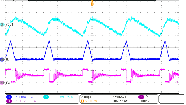
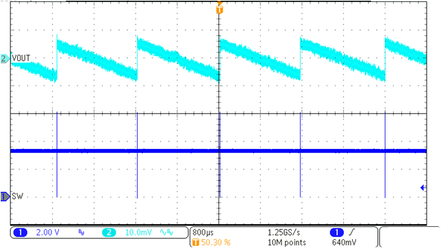
VIN = 6 V L = 2.2 μH Fsw = 1.0 MHz
VOUT = 3.3 V IOUT = 100 mA Auto PFM/PWM
Figure 9-76 Output Voltage Ripple
GUID-20221011-SS0I-PQLQ-3481-WRB35VH7JTZR-low.png
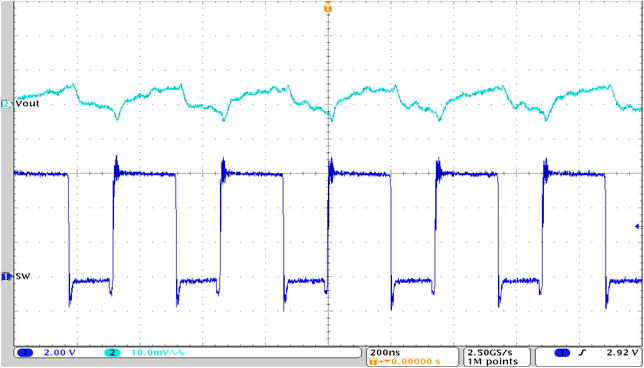
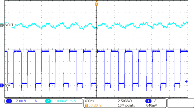
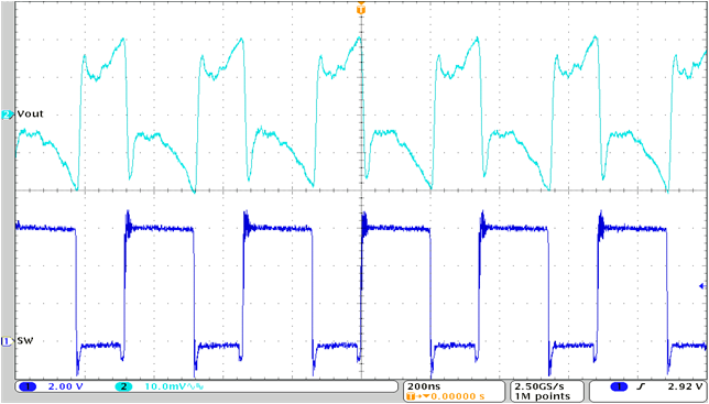
VIN = 6 V L = 1.0 μH Fsw = 2.5 MHz
VOUT = 3.3 V IOUT = 3 A FPWM
Figure 9-78 Output Voltage Ripple
GUID-20221011-SS0I-QWCN-M0CS-JDBVQG61VGXQ-low.png
VIN = 6 V L = 2.2 μH Fsw = 1.0 MHz
VOUT = 3.3 V IOUT = 5 A FPWM
Figure 9-80 Current Limit
GUID-20220812-SS0I-7CQV-X4BH-MLG0FFSN0G5V-low.svg
VOUT = 3.3 V L = 1.0 μH Fsw = 2.5 MHz
Forced PWM
Figure 9-53 Efficiency vs Output Current
GUID-20220816-SS0I-RSKZ-JQDZ-K3XJVVKGDSDS-low.svg
VOUT = 3.3 V L = 1.0 μH Fsw = 2.5 MHz
Forced PWM
Figure 9-55 Switching Frequency vs Input Voltage
GUID-20220816-SS0I-44TP-NL9C-HLSB4MFZWRP1-low.svg
VOUT = 3.3 V L = 1.0 μH Fsw = 2.5 MHz
Forced PWM
Figure 9-57 Output Voltage vs Output Current
GUID-20220812-SS0I-FLRN-BMLK-TZJTQSN9CDD9-low.svg
VOUT = 3.3 V L = 2.2 μH Fsw = 1.0 MHz
Forced PWM
Figure 9-59 Efficiency vs Output Current
GUID-20220816-SS0I-CLWH-XGQV-BQGPD9LMH6LV-low.svg
VOUT = 3.3 V L = 2.2 μH Fsw = 1.0 MHz
Forced PWM
Figure 9-61 Switching Frequency vs Input Voltage
GUID-20220816-SS0I-DCTD-J9RH-GMFQ9B73QVNF-low.svg
VOUT = 3.3 V L = 2.2 μH Fsw = 1.0 MHz
Forced PWM
Figure 9-63 Output Voltage vs Output Current
GUID-20221011-SS0I-LDJK-7CLP-RVBNGVXJN7VD-low.png
VIN = 6 V Css = 0 nF Fsw = 2.5 MHz
VOUT = 3.3 V IOUT = 0 A Auto PFM/PWM
Figure 9-65 Start-Up Timing
GUID-20221011-SS0I-N286-NKJJ-KL7NKZBDZDFK-low.png
VIN = 6 V Css = 0 nF Fsw = 2.5 MHz
VOUT = 3.3 V IOUT = 3 A FPWM
Figure 9-67 Start-Up Timing
GUID-20221011-SS0I-NP7K-9WC9-QJRGQ5JRWLBX-low.png
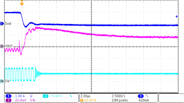
VIN = 6 V L = 1.0 μH Fsw = 2.5 MHz
VOUT = 3.3 V IOUT = 10 mA Auto PFM/PWM
Figure 9-69 Shutdown Timing with Output Discharge Enabled
GUID-20221011-SS0I-TFP7-DPPL-MFKD2G959D5L-low.png
VIN = 6 V L = 1.0 μH Fsw = 2.5 MHz
VOUT = 3.3 V IOUT = 3 A FPWM
Figure 9-71 Shutdown Timing with Output Discharge Disabled
GUID-20221011-SS0I-C56R-FXLL-L0K3WNP4WPNF-low.png
VIN = 6 V L = 1.0 μH Fsw = 2.5 MHz
VOUT = 3.3 V IOUT = 10 mA to 1 A Auto PFM/PWM
Figure 9-73 Load Transient Response Undershoot
GUID-20221011-SS0I-DLL2-FCLW-FDJ51BCBWKSJ-low.png
VIN = 6 V L = 1.0 μH Fsw = 2.5 MHz
VOUT = 3.3 V IOUT = 0 A Auto PFM/PWM
Figure 9-75 Output Voltage Ripple
GUID-20221011-SS0I-ZXQ5-FWWZ-1ZJWRM39HHJP-low.png
VIN = 6 V L = 1.0 μH Fsw = 2.5 MHz
VOUT = 3.3 V IOUT = 1 A Auto PFM/PWM
Figure 9-77 Output Voltage Ripple
GUID-20221011-SS0I-HC89-2NZS-WK8DVX1RTHLT-low.png
VIN = 6 V L = 1.0 μH Fsw = 2.5 MHz
VOUT = 3.3 V IOUT = 3 A FPWM
Figure 9-79 Input Voltage Ripple
GUID-20221011-SS0I-DVRK-RM90-D57WWDDTNPHX-low.svg
VIN = 6 V L = 1.0 μH Fsw = 2.5 MHz
VOUT = 3.3 V IOUT = 3 A FPWM
Figure 9-81 Bode Plot