SLVSAM8D July   2013  – August 2019 TPS63050 , TPS63051

PRODUCTION DATA.  

  1. Features
  2. Applications
  3. Description
    1.     Device Images
      1.      Simplified Schematic (WCSP)
      2.      Efficiency vs Output Current
  4. Revision History
  5. Device Comparison Table
  6. Pin Configuration and Functions
    1.     Pin Functions
  7. Specifications
    1. 7.1 Absolute Maximum Ratings
    2. 7.2 ESD Ratings
    3. 7.3 Recommended Operating Conditions
    4. 7.4 Thermal Information
    5. 7.5 Electrical Characteristics
    6. 7.6 Switching Characteristics
    7. 7.7 Typical Characteristics
  8. Detailed Description
    1. 8.1 Overview
    2. 8.2 Functional Block Diagrams
    3. 8.3 Feature Description
      1. 8.3.1 Power Good
      2. 8.3.2 Overvoltage Protection
      3. 8.3.3 Undervoltage Lockout (UVLO)
      4. 8.3.4 Thermal Shutdown
      5. 8.3.5 Soft Start
      6. 8.3.6 Short Circuit Protection
    4. 8.4 Device Functional Modes
      1. 8.4.1 Control Loop Description
      2. 8.4.2 Power Save Mode Operation
      3. 8.4.3 Adjustable Current Limit
      4. 8.4.4 Device Enable
  9. Application and Implementation
    1. 9.1 Application Information
    2. 9.2 Typical Application
      1. 9.2.1 Design Requirements
      2. 9.2.2 Detailed Design Procedure
        1. 9.2.2.1 Custom Design With WEBENCH® Tools
        2. 9.2.2.2 Output Filter Design
        3. 9.2.2.3 Inductor Selection
        4. 9.2.2.4 Capacitor selection
          1. 9.2.2.4.1 Input Capacitor
          2. 9.2.2.4.2 Output Capacitor
        5. 9.2.2.5 Setting the Output Voltage
      3. 9.2.3 Application Curves
  10. 10Power Supply Recommendations
  11. 11Layout
    1. 11.1 Layout Guidelines
    2. 11.2 Layout Example (WCSP)
    3. 11.3 Layout Example (HotRod)
    4. 11.4 Thermal Considerations
  12. 12Device and Documentation Support
    1. 12.1 Custom Design With WEBENCH® Tools
    2. 12.2 Device Support
      1. 12.2.1 Third-Party Products Disclaimer
    3. 12.3 Related Links
    4. 12.4 Receiving Notification of Documentation Updates
    5. 12.5 Community Resources
    6. 12.6 Trademarks
    7. 12.7 Electrostatic Discharge Caution
    8. 12.8 Glossary
  13. 13Mechanical, Packaging, and Orderable Information

Package Options

Mechanical Data (Package|Pins)
Thermal pad, mechanical data (Package|Pins)
Orderable Information

Application Curves

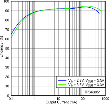
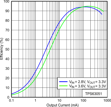
TPS63050 TPS63051 Figure13_SLVSAM8.gif
PFM/PWM = Low VOUT = 3.3 V
Figure 10. Efficiency vs Output Current
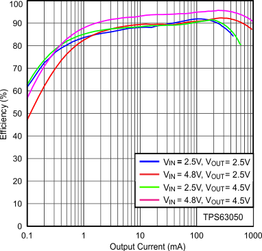
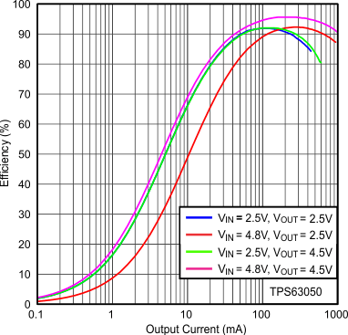
TPS63050 TPS63051 Figure15_SLVSAM8.gif
PFM/PWM = Low VOUT = 2.5 V, 4.5 V
Figure 12. Efficiency vs Output Current
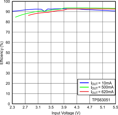
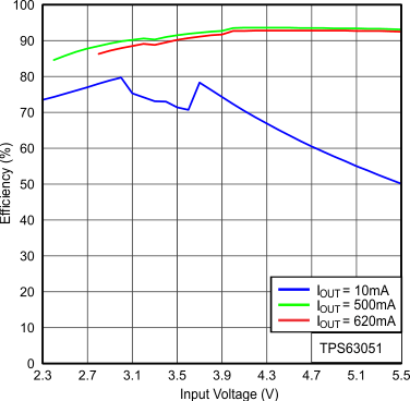
TPS63050 TPS63051 Figure17_SLVSAM8.gif
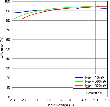
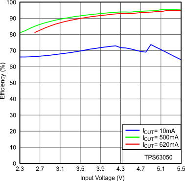
PFM/PWM = Low VOUT= 3.3 V
Figure 14. Efficiency vs Input Voltage
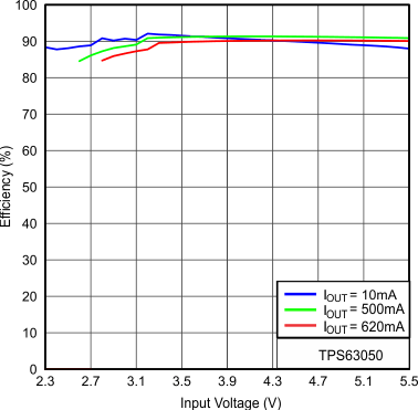
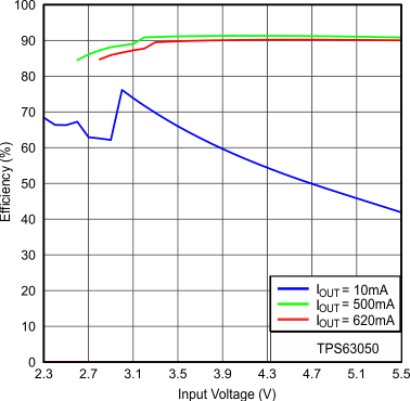
TPS63050 TPS63051 Figure19_SLVSAM8.gif
PFM/PWM = Low VOUT = 2.5 V
Figure 16. Efficiency vs Input Voltage
TPS63050 TPS63051 Figure21_SLVSAM8.gif
PFM/PWM = Low VOUT = 4.5 V
Figure 18. Efficiency vs Input Voltage
TPS63050 TPS63051 Figure23_SLVSAM8.gif
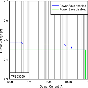
VIN = 2.5 V
Figure 20. Output Voltage vs Output Current
TPS63050 TPS63051 Figure25_SLVSAM8.gif
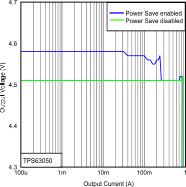
VIN = 4.5 V
Figure 22. Output Voltage vs Output Current
TPS63050 TPS63051 Figure27_SLVSAM8.gif
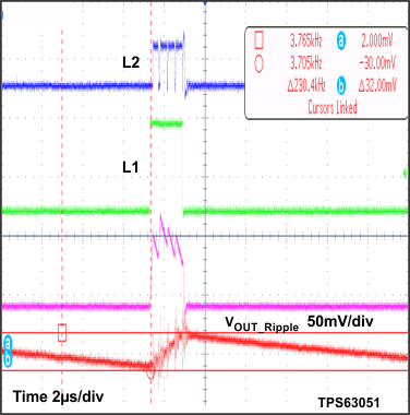
VIN = 2.8 V IOUT = 16 mA
Figure 24. Output Voltage Ripple in Boost Mode and PFM to PWM Transition
TPS63050 TPS63051 Figure29_SLVSAM8.gif
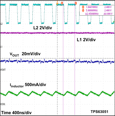
VIN = 2.5 V IOUT = 300 mA
Figure 26. Switching Waveform in Boost Mode and PWM
TPS63050 TPS63051 Figure31_SLVSAM8.gif
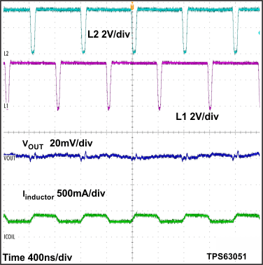
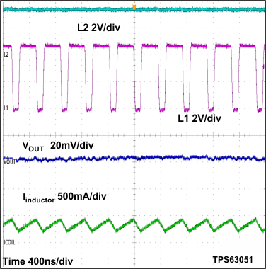
VIN = 3.4 V IOUT = 300 mA
Figure 28. Switching Waveform in Buck-Boost Mode and PWM
TPS63050 TPS63051 Figure33_SLVSAM8.gif
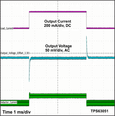
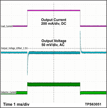
VIN = 3.6 V Load change from 0 mA to 300 mA
Figure 30. Load Transient Response
TPS63050 TPS63051 Figure35_SLVSAM8.gif
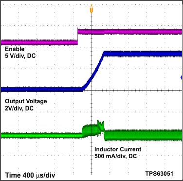
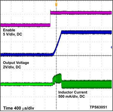
VOUT = 3.3 V VIN = 2.5 V IOUT = 0 mA
Figure 32. Start Up After Enable
TPS63050 TPS63051 Figure14_SLVSAM8.gif
PFM/PWM = High VOUT = 3.3 V
Figure 11. Efficiency vs Output Current
TPS63050 TPS63051 Figure16_SLVSAM8.gif
PFM/PWM = High VOUT = 2.5 V, 4.5 V
Figure 13. Efficiency vs Output Current
TPS63050 TPS63051 Figure18_SLVSAM8.gif
PFM/PWM = High VOUT= 3.3 V
Figure 15. Efficiency vs Input Voltage
TPS63050 TPS63051 Figure20_SLVSAM8.gif
PFM/PWM = High VOUT = 2.5 V
Figure 17. Efficiency vs Input Voltage
TPS63050 TPS63051 Figure22_SLVSAM8.gif
PFM/PWM =High VOUT= 4.5 V
Figure 19. Efficiency vs Input Voltage
TPS63050 TPS63051 Figure24_SLVSAM8.gif
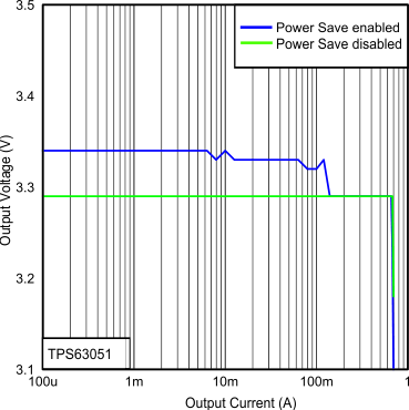
VIN = 3.3 V
Figure 21. Output Voltage vs Output Current
TPS63050 TPS63051 Figure26_SLVSAM8.gif
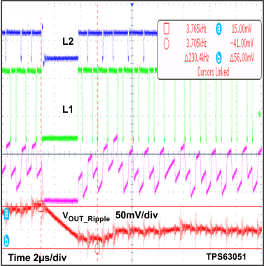
VIN = 3.3 V IOUT = 145 mA
Figure 23. Output Voltage ripple in Buck-Boost mode and PFM to PWM transition
TPS63050 TPS63051 Figure28_SLVSAM8.gif
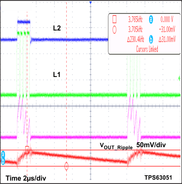
VIN = 4.2 V IOUT = 16 mA
Figure 25. Output Voltage Ripple in Buck Mode and PFM to PWM Transition
TPS63050 TPS63051 Figure30_SLVSAM8.gif
VIN = 4.5 V IOUT = 300 mA
Figure 27. Switching Waveform in Buck Mode and PWM
TPS63050 TPS63051 Figure32_SLVSAM8.gif
VIN = 2.8 V Load change from 0 mA to 300 mA
Figure 29. Load Transient Response
TPS63050 TPS63051 Figure34_SLVSAM8.gif
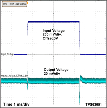
VOUT = 3.3 V IOUT = 500 mA
Figure 31. Line Transient Response
TPS63050 TPS63051 Figure36_SLVSAM8.gif
VOUT = 3.3 V VIN = 4.2 V IOUT = 0 mA
Figure 33. Start Up After Enable