SLVSA92C November 2011 – September 2020 TPS63060 , TPS63061
PRODUCTION DATA
- 1 Features
- 2 Applications
- 3 Description
- 4 Revision History
- 5 Device Comparison
- 6 Pin Configuration and Functions
- 7 Specifications
- 8 Detailed Description
- 9 Application and Implementation
- 10Power Supply Recommendations
- 11Layout
- 12Device and Documentation Support
- 13Mechanical, Packaging, and Orderable Information
Package Options
Mechanical Data (Package|Pins)
- DSC|10
Thermal pad, mechanical data (Package|Pins)
- DSC|10
Orderable Information
3 Description
The TPS6306x devices provide a power supply solution for products powered by either three-cell up to six-cell alkaline, NiCd or NiMH battery, or a one-cell or dual-cell Li-Ion or Li-polymer battery. Output currents can go as high as 2 A while using a dual-cell Li-Ion or Li-polymer battery, and discharge to 5 V or lower. The buck-boost converter is based on a fixed frequency, pulse width modulation (PWM) controller using synchronous rectification to obtain maximum efficiency. At low load currents, the converter enters power save mode to maintain high efficiency over a wide load current range. The power save mode can be disabled, forcing the converter to operate at a fixed switching frequency. The maximum average current in the switches is limited to a typical value of 2.25 A. The output voltage is programmable using an external resistor divider, or is fixed internally on the chip. The converter can be disabled to minimize battery drain. During shutdown, the load disconnects from the battery.
The devices are available in a 3 mm × 3 mm, 10-pin, WSON (DSC) package.
| PART NUMBER | PACKAGE | BODY SIZE (NOM) |
|---|---|---|
| TPS63060 | WSON (10) | 3.00 mm × 3.00 mm |
| TPS63061 |
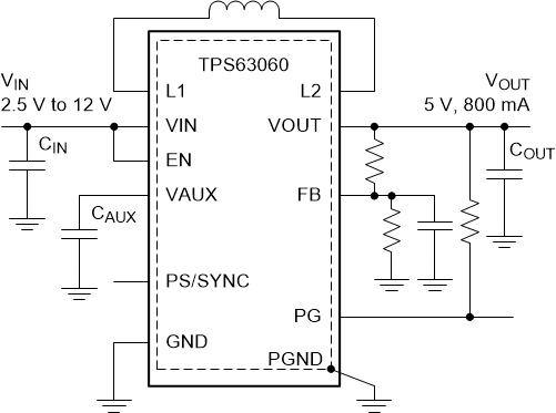
 Simplified Application
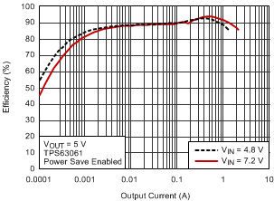
 Efficiency vs Output Current