SLVSA92C November   2011  – September 2020 TPS63060 , TPS63061

PRODUCTION DATA  

  1. Features
  2. Applications
  3. Description
  4. Revision History
  5. Device Comparison
  6. Pin Configuration and Functions
    1.     Pin Functions
  7. Specifications
    1. 7.1 Absolute Maximum Ratings
    2. 7.2 ESD Ratings
    3. 7.3 Recommended Operating Conditions
    4. 7.4 Thermal Information
    5. 7.5 Electrical Characteristics
    6. 7.6 Typical Characteristics
  8. Detailed Description
    1. 8.1 Overview
    2. 8.2 Functional Block Diagrams
    3. 8.3 Feature Description
      1. 8.3.1 Power Good
      2. 8.3.2 Soft-Start Function
      3. 8.3.3 Short-Circuit Protection
      4. 8.3.4 Overvoltage Protection
      5. 8.3.5 Undervoltage Lockout
      6. 8.3.6 Overtemperature Protection
    4. 8.4 Device Functional Modes
      1. 8.4.1 Buck-Boost Operation
      2. 8.4.2 Control Loop
      3. 8.4.3 Power-Save Mode
      4. 8.4.4 Synchronization
      5. 8.4.5 Dynamic Voltage Positioning
      6. 8.4.6 Dynamic Current Limit
      7. 8.4.7 Device Enable
  9. Application and Implementation
    1. 9.1 Application Information
    2. 9.2 Typical Application
      1. 9.2.1 Design Requirements
      2. 9.2.2 Detailed Design Procedure
        1. 9.2.2.1 Step One: Output Filter Design
        2. 9.2.2.2 Step Two: Inductor Selection
        3. 9.2.2.3 Step Three: Capacitor Selection
          1. 9.2.2.3.1 Input Capacitors
          2. 9.2.2.3.2 Output Capacitor
          3. 9.2.2.3.3 Bypass Capacitor
        4. 9.2.2.4 Step Four: Setting the Output Voltage
      3. 9.2.3 Application Curves
  10. 10Power Supply Recommendations
  11. 11Layout
    1. 11.1 Layout Guidelines
    2. 11.2 Layout Example
  12. 12Device and Documentation Support
    1. 12.1 Device Support
      1. 12.1.1 Development Support
    2. 12.2 Documentation Support
      1. 12.2.1 Related Documentation
    3. 12.3 Receiving Notification of Documentation Updates
    4. 12.4 Community Resources
    5. 12.5 Trademarks
  13. 13Mechanical, Packaging, and Orderable Information

Package Options

Mechanical Data (Package|Pins)
Thermal pad, mechanical data (Package|Pins)
Orderable Information

Dynamic Current Limit

The dynamic current limit function maintains the output voltage regulation when the power source becomes weaker. The maximum current allowed through the switch depends on the voltage applied at the input terminal of the TPS6306x devices. Figure 8-5 shows this dependency, and the ISW vs VIN. The dynamic current limit has its lowest value when reaching the minimum recommended supply voltage at VIN.

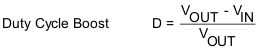
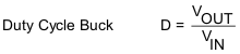
Given the ISW value from Figure 8-5, is then possible to calculate the output current reached in boost mode using Equation 1 and Equation 2 and in buck mode using Equation 3 and Equation 4.

Equation 1. GUID-5A78B0CF-419B-468C-A97B-0CCDA64D6744-low.gif
Equation 2. GUID-C7929BA9-D0D9-4118-A8E0-C21D77711FD4-low.gif
Equation 3. GUID-81D0CA2C-E794-4D5B-8BFD-4AFE771D2D1D-low.gif
Equation 4. GUID-3FDCF2ED-58D0-4778-967F-4B8C6400CC4F-low.gif

where

  • η is the estimated converter efficiency (use the number from the efficiency curves or 0.80 as an assumption)
  • f is the converter switching frequency (typical 2.4 MHz)
  • L is the selected inductor value

If the die temperature increases above the recommended maximum temperature, the dynamic current limit becomes active. The current limit is reduced with temperature increasing.

GUID-14D8BCD8-2C8C-456C-86B0-EAC0F9E4198A-low.gifFigure 8-5 Average Inductance Current vs Input Voltage